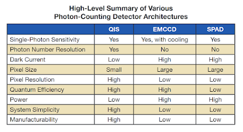
Image Sensors World Go to the original article...
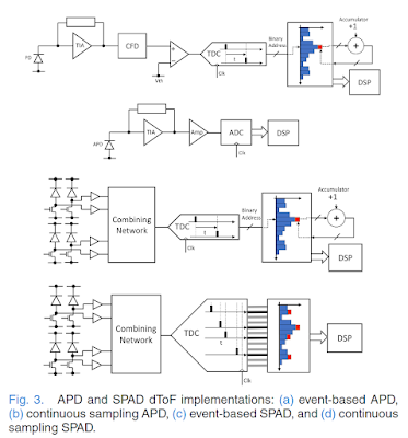
In a recent preprint (https://arxiv.org/pdf/2209.11772.pdf) Gyongy et al. describe a new 64x32 SPAD-based direct time-of-flight sensor with in-pixel histogramming and processing capability.
Abstract
3D flash LIDAR is an alternative to the traditional scanning LIDAR systems, promising precise depth imaging in a compact form factor, and free of moving parts, for applications such as self-driving cars, robotics and augmented reality (AR). Typically implemented using single-photon, direct time-of-flight (dToF) receivers in image sensor format, the operation of the devices can be hindered by the large number of photon events needing to be processed and compressed in outdoor scenarios, limiting frame rates and scalability to larger arrays. We here present a 64 × 32 pixel (256 × 128 SPAD) dToF imager that overcomes these limitations by using pixels with embedded histogramming, which lock onto and track the return signal. This reduces the size of output data frames considerably, enabling maximum frame rates in the 10 kFPS range or 100 kFPS for direct depth readings. The sensor offers selective readout of pixels detecting surfaces, or those sensing motion, leading to reduced power consumption and off-chip processing requirements. We demonstrate the application of the sensor in mid-range LIDAR.