Image Sensors World Go to the original article...
Trioptics sent me its presentation at Autosens Brussels 2020 about LiDAR optics alignment:LiDAR News: Trioptics, ADI, Leddar, Innoviz, Luminar
Breaking Si Pixel Speed Limit
Image Sensors World Go to the original article...
MDPI paper "Toward the Super Temporal Resolution Image Sensor with a Germanium Photodiode for Visible Light" by Nguyen Hoai Ngo, Anh Quang Nguyen, Fabian M. Bufler, Yoshinari Kamakura, Hideki Mutoh, Takayoshi Shimura, Takuji Hosoi, Heiji Watanabe, Philippe Matagne, Kazuhiro Shimonomura, Kohsei Takehara, Edoardo Charbon, and Takeharu Goji Etoh from Ritsumeikan University, Hanoi University of Science and Technology, IMEC, Osaka Institute of Technology, Osaka University, Link Research Corporation, Kindai University, and EPFL presents Ge PD to overcome the Si speed limit:
"The theoretical temporal resolution limit tT of a silicon photodiode (Si PD) is 11.1 ps. We call “super temporal resolution” the temporal resolution that is shorter than that limit. To achieve this resolution, Germanium is selected as a candidate material for the photodiode (Ge PD) for visible light since the absorption coefficient of Ge for the wavelength is several tens of times higher than that of Si, allowing a very thin PD. On the other hand, the saturation drift velocity of electrons in Ge is about 2/3 of that in Si. The ratio suggests an ultra-short propagation time of electrons in the Ge PD. However, the diffusion coefficient of electrons in Ge is four times higher than that of Si. Therefore, Monte Carlo simulations were applied to analyze the temporal resolution of the Ge PD. The estimated theoretical temporal resolution limit is 0.26 ps, while the practical limit is 1.41 ps. To achieve a super temporal resolution better than 11.1 ps, the driver circuit must operate at least 100 GHz. It is thus proposed to develop, at first, a short-wavelength infrared (SWIR) ultra-high-speed image sensor with a thicker and wider Ge PD, and then gradually decrease the size along with the progress of the driver circuits."
Fairchild Imaging Starts Sampling its 3rd Generation sCMOS Sensor with 0.5e- Read Noise, Demos Imaging at 0.0007 Lux Illumination
Image Sensors World Go to the original article...
While BAE Fairchild Imaging has announced the HWK4123 sensor in February, its sampling starts just now:Trinamix Molecular Sensing for Smartphones
Image Sensors World Go to the original article...
VentureBeat publishes an article on Trinamix intention to enter smartphone market with its multispectral sensors for materials identification:
"The technology is called near-infrared spectroscopy, and it uses laser light to detect the molecular vibrations that distinguish different substances.
Trinamix said it intends to build a potent, yet miniaturized infrared sensing module for integration into smartphones. The module sends out infrared light, which is reflected from the object and detected by the sensor. The company said breakthroughs in research enabled it to reduce the size of the device down to a smartphone form factor while ensuring high-volume production capacities."
Metalens Paper
Image Sensors World Go to the original article...
APL Photonics paper "CMOS-compatible all-dielectric metalens for improving pixel photodetector arrays" by E. Mikheeva, J.-B. Claude, M. Salomoni, J. Wenger, J. Lumeau, R. Abdeddaim, A. Ficorella, A. Gola, G. Paternoster, M. Paganoni, E. Auffray, P. Lecoq, and S. Enoch from Institut Fresnel, Multiwave Imaging, University of Milano-Bicocca, CERN, FBK, and Multiwave Metacrystal SA proposes an improvement in SPAD array sensitivity:
"Metasurfaces and, in particular, metalenses have attracted large interest and enabled various applications in the near-infrared and THz regions of the spectrum. However, the metalens design in the visible range stays quite challenging due to the smaller nanostructuring scale and the limited choice of lossless CMOS-compatible materials. We develop a simple yet efficient design of a polarization-independent, broadband metalens suitable for many CMOS-compatible fabrication techniques and materials and implement it for the visible spectral range using niobium pentoxide (Nb2O5). The produced metalens demonstrates high transmittance and focusing ability as well as a large depth of focus, which makes it a promising solution for a new generation of silicon photomultiplier photodetectors with reduced fill factor impact on the performance and reduced electron–hole generation regions, which altogether potentially leads to improved photodetection efficiency and other characteristics."
Qualcomm’s Spectra 580 ISP: The Future of Photography?
Image Sensors World Go to the original article...
Qualcomm unveils the its latest triple ISP at 2020 Tech Summit:
Samsung Compares DTI with Skyscrapers, Promises 0.6X um Pixel Soon
Image Sensors World Go to the original article...
The recent Samsung Investor Forum presentation from Nov 24, 2020 by System LSI Group EVP Park Yong-in shows the company's plans to introduce 0.6X um pixel and compares its DTI aspect ratio with skyscrapers:Samsung Compares DTI with Skyscrapers, Promises 0.6X um Pixel Soon
Image Sensors World Go to the original article...
The recent Samsung Investor Forum presentation from Nov 24, 2020 by System LSI Group EVP Park Yong-in shows the company's plans to introduce 0.6X um pixel and compares its DTI aspect ratio with skyscrapers:Terabee Introduction to ToF Sensing
Image Sensors World Go to the original article...
Terabee publishes a video explaining ToF principles:
GPixel Expands 2.5um GS Family with 18MP Sensor
Image Sensors World Go to the original article...
Gpixel expands the C-Mount GMAX product family with the GMAX2518, a 1” format Global Shutter CMOS sensor for industrial applications. The sensor is designed around the proven 2.5 µm charge domain global shutter pixel, provides 4508(H) x 4096(V) resolution (18 MP), and supports up to 64fps with 12bit output and 150fps with 10bit output.The 2.5 um pixel achieves a FWC of 8k e-, read noise less than 2 e- and maximum DR of 66dB. The sensor provides a peak QE of 65%, a PLS of -80dB.
With an outer dimension of 20.8 mm x 19.5 mm, GMAX2518’s 226-pin LGA ceramic package is designed to fit easily into a standard 29 mm x 29 mm camera housing.
“We are excited to offer customers another sensor in this very popular 2.5um-pixel family, now
supporting 4 unique cameras from only 1 hardware design. The expansion of Gpixel’s line up of C-mount compatible global shutter sensors empowers our customers to develop a broad portfolio of high performance cameras in the most resource efficient and cost effective way possible. This product is part of our fast growing GMAX product family, which we will continue to expand in the near future to help our customers make the most of their investment in Gpixel,” says Wim Wuyts, CCO of Gpixel.
GMAX2518 engineering samples can be ordered now for delivery in December 2020.
ST Claims #1 Position in ToF Sensors
Image Sensors World Go to the original article...
ST publishes an investor presentation on its AMS (Analog, MEMS & Sensors) Group's business positioning itself as #1 ToF company:
Digitimes on Sony CIS Business
Image Sensors World Go to the original article...
Digitimes Research reviews recent Sony CIS sales forecasts:
Sony CIS "sales for fiscal 2020 (April 2020-March 2021) to fall 11.8% on year compared to a 6.5% decline estimated earlier, due mainly to slackened demand for handset applications as global handset sales are projected to shrink by 10% in 2020, according to Digitimes Research.
...the estimated sales shrinkage will lead to an on-year reduction of 65.6% in fiscal 2020 operating incomes for the I&SS unit.
Sony has cut its budget for a three-year investment plan ending March 2021 by 12.9% to JPY610 billion (US$5.84 billion) from JPY700 billion. It is also actively exploring new clients to offset the loss of orders from Huawei, and developing AI-enabled CIS products in cooperation with Microsoft to boost competitiveness in the market, while also contracting TSMC to fabricate 3D-stacked image signal processors, according to Digitimes Research."
Samsung Sued by Pictos Over Patent Infringement
Image Sensors World Go to the original article...
KoreaTimes: Samsung is facing the U.S. International Trade Commission's (USITC) investigation for allegedly infringing on image sensor patents held by Pictos Technologies. This is a fairly long story publicly presented in 2018 by Gil Amelio.
It's not clear what is the relation between the new Pictos and the old image sensor company under the same name that started as Rockwell spin-off and later acquired by ESS. Bloomberg reports that the new Pictos has been formerly known as Imperium IP.
UBS: iPhone 12 Pro 3D Cameras Cost 67% of 2D Cameras
Image Sensors World Go to the original article...
IFNews quotes UBS and Fomalhaut teardown analysis estimating 3D cameras in iPhone 12 Pro and Pro Max cost at 67% and 54% of the cost of 2D cameras, respectively:
UBS poll reveals that smartphone camera spec is rated #12 among the most desirable features. Other image sensor-based features like dual camera, on-display fingerprint, Face ID, and AR/VR functionality are all rated much lower than that:
Sony SLVS-EC Article
Image Sensors World Go to the original article...
Sony publishes an article on its image sensor interface Scalable Low-Voltage Signaling with Embedded Clock, abbreviated SLVS-EC. SLVS-EC is standardized by the Japan Industrial Imaging Association (JIIA). It looks similar to MIPI M-PHY, but has a slower speed of up to 5Gbps per lane.
Sony Releases 5um Pixel VGA ToF Sensor
Image Sensors World Go to the original article...
Sony releases a new 5um BSI ToF sensor - 5um pixel-based IMX570. The new VGA sensor is sampling now with mass production start planned for March 2021.
Sony Releases 5um Pixel VGA ToF Sensor
Image Sensors World Go to the original article...
Sony releases a new 5um BSI ToF sensor - 5um pixel-based IMX570. The new VGA sensor is sampling now with mass production start planned for March 2021.
Sony Buys Hundreds of Intel Patents
Image Sensors World Go to the original article...
IPNewsShots reports that Sony has bought hundreds of Intel patents to protect its image sensor business. Earlier, Sony also has quietly acquired IBM semiconductor patents.
iPhone 12 Teardown
Image Sensors World Go to the original article...
Nikkei and Fomalhaut Techno Solutions tore down the iPhone 12 and iPhone 12 Pro and checked the components origins:iToF Phase Unwrapping Review
Image Sensors World Go to the original article...
Chronoptics CTO Refael Whyte publishes an overview of approaches to "Phase Wrapping and its Solution for Indirect Time-of-Flight Depth Sensing" with very nice animations:
Characterization of CIS Noise for Automotive Applications
Image Sensors World Go to the original article...
Institute of Technology Sligo and Waterford Institute of Technology, Irland, publishe a paper "Characterisation of CMOS Image Sensor Performance in Low Light Automotive Applications" by Shane Gilroy, John O'Dwyer, and Lucas Bortoleto.
SmartSens Sales Doubled this Year, Expected to Double Again Next Year, IPO Plans
Image Sensors World Go to the original article...
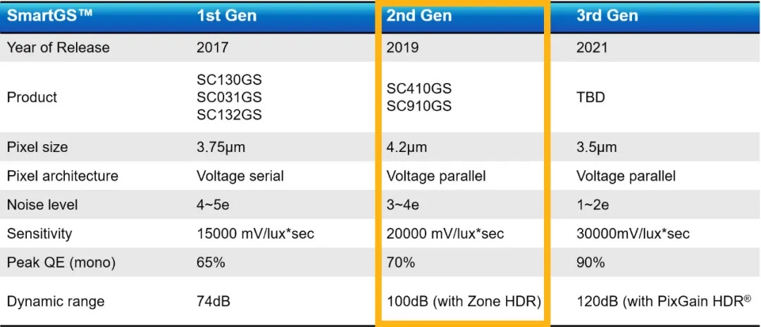
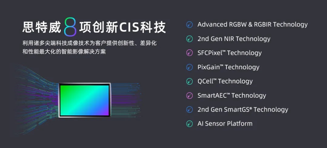
Smartsens has held a Partnership Meeting 2020 (SPM 2020) updating about the company's business and future plans. Smartsens CEO Xu Chen says:
"2020 is an unusual year, but under the influence of the complex international situation and the global epidemic, the overall CIS industry still maintains a growth rate of 20% (data source: Yole)
Dr. Xu Chen pointed out that although next year’s forecasted growth rate has slowed down, Smartsens' overall sales situation still maintains a high-speed growth, and has doubled sales this year, with shipments reaching 220 million units. It is expected that the target set at the beginning of the year will be exceeded, and the sales target of Smartsens will double again next year.
In addition to the repeated increase in sales, Smartsens product line and application areas are also rapidly expanding. The number of Tapeout products has doubled from 13 in 2019 to 26 in 2020, and strives to empower more with excellent CIS imaging technology.
Smartsens' consumer-grade Global Shutter image sensor market, which was laid out in 2017, also achieved good results this year, ranking first in the world in terms of shipments in the consumer-grade machine vision field . And this year's acquisition of Allchip (Shenzhen Anxin Micro) also enabled Smartsens to quickly enter the automotive electronics application field . In addition, just before the SPM 2020 conference, Smartsens released a full range of 2MP-13MP Cellphone Sensor (CS) series of mobile phone application products , officially entering the mobile phone market.
Mr. Chen Xu, Deputy Director of TSMC, gave a speech introducing TSMC’s current latest process R&D and production capacity planning, and said that TSMC will spare no effort to cooperate with Smartsens' growth and development, and also strongly support Smartsens production capacity manufacturing. In the future, TSMC will also work with Smartsens to help China's semiconductor industry chain achieve global cutting-edge quality and maintain a state of sustainable development.
Samsung Semiconductor Executive (Vice President) Mr. Minghui Zhu said in his speech that the cooperation between Samsung and Smartsens is very harmonious and happy, and highly summarized and appreciated the development of Smartsens in recent years with three characteristics. The first is "speed". , I am deeply impressed by Smartsens’s high efficiency; the second is "high and big ", which greatly appreciates its technological innovation ability, and the third is "strategic vision . In the future, Samsung will continue to make efforts to support Smartsens' strategic development and look forward to more future results of joint development with Smartsens.
Next year, Smartsens will celebrate its 10th birthday. On this conference, Dr. Xu Chen announced the three major events of Smarsens' 10th anniversary to the guests. These include the spacious and bright brand-new Smartsens office building that is under design and renovation and will be settled in April next year ; and the new Kunshan test center with a capacity plan of 100kk/month and an area of 20 acres that will be completed next year; However, after completing the 1.5 billion pre-ipo round of financing this year, Smartsens will submit a listing application and start the listing plan!"
Hole in Pixel Improves NIR Response
Image Sensors World Go to the original article...
W&WSens Devices, University California at Davis, and University California at Santa Cruz publish a paper "Single Microhole per Pixel in CMOS Image Sensor with Enhanced Optical Sensitivity in Near-Infrared" by E. Ponizovskaya Devine, Wayesh Qarony, Ahasan Ahamed, Ahmed S Mayet, Soroush Ghandiparsi, Cesar Bartolo-Perez, Aly F Elrefaie, Toshishige Yamada, Shih-Yuan Wang, and M. Saif Islam.Infineon Anticipates ToF Camera to Become Standard Feature in Smartphones
Image Sensors World Go to the original article...
SemiconductorForYou publishes an interview with Philipp von Schierstaedt, SVP RF & Sensors at Infineon. Few quotes:
"We see a development towards 3D ToF image sensors as a standard for high-end smartphones on the front camera – flagship phones are already proving this – and on the rear camera. The fastest growing will surely be the rear camera with above 500 million units/y over the next years. The deployment of 3D sensing technologies will follow this growth as they solve the challenges that new applications set to the rear camera and that traditional 2D technologies fail to accomplish: a real 3D depth map.
Still, challenges exist, for example current commercial devices deploying existing 3D image sensing solutions are not yet able to provide a reasonable resolution without significant trade-offs on extended distance ranges and on the power consumption.
Such shortcomings are now being addressed by the latest 3D ToF imager generations in the REAL3 portfolio of Infineon. Therefore we’re convinced that we will see our new 3D sensor either enabling new classes of applications or taking existing applications to a new level of quality and user experience."
Draper Si-Ge-based Single-Photon Detector Gets Award
Image Sensors World Go to the original article...
Draper reports that its Single Photon Detector (SPD) patent has been awarded by by the Boston Patent Law Association at its 10th Annual Invented Here! event.
Draper’s SPD is intended to be configured in an array of multiple SPDs capable of detecting a single photon with high timing resolution, speed and efficiency over an unparalleled wavelength range, from visible to infrared.
Draper’s SPD uses a silicon-germanium photodiode, which enables detection of the longer wavelengths of light and performance similar to a conventional silicon SPD. It can also function at room temperature. The performance of the new detector is intended to enable ultralow dark-counting rate and timing resolution of better than one nanosecond.
Steven Spector, principal member of Draper’s technical staff, developed the technology with a team at Draper. He said, “Draper’s SPD is so fast and efficient that it can absorb and detect a single particle of light and reset itself for the next one within a nanosecond.”
The patent US10636918 "Single electron transistor triggered by photovoltaic diode" presents the idea using a single electron bipolar avalanche transistor (SEBAT) circuit:
"Embodiments of the present invention are directed to a single photon detec