Image Sensors World Go to the original article...
SystemPlus publishes a reverse engineering report "3D Time-of-Flight Module in Meizu 17 Pro."
Visual Industry Guide
Image Sensors World Go to the original article...
SystemPlus publishes a reverse engineering report "3D Time-of-Flight Module in Meizu 17 Pro."
Image Sensors World Go to the original article...
MIRAE Asset publishes few slides with the CIS market data:
Image Sensors World Go to the original article...
BusinessWire: Starting from security and surveillance sensors, Smartsens has recently expanded into automotive applications. Now, the company announces plans to penetrate smartphone image sensor market with the CS (Cellphone Sensor) Series products—including the SC200CS-mono, SC200CS-color, SC500CS, SC800CS, and SC1300CS/SC1301CS—covering a range of 2MP to 13MP resolutions to meet a diverse set of applications and customers.
SmartSens is leveraging its proprietary SFCPixel Technology and ultra-low noise reading circuit design in its new smartphone sensors, borrowing from its years of experience in developing superior night vision imaging technology for security devices. These technologies effectively improve performance in low-light environments, allowing smartphone cameras to capture rich and vibrant images under extremely challenging conditions.
The new CS series deliver excellent signal-to-noise ratio. For example, the SC500CS reduces reading noise by over 30% compared with products of the same specifications in the industry while the fixed noise of SC800CS is significantly reduced by 72% with the Max SNR increased by 3dB compared to similar products. Coupled with the signal-to-noise ratio, the noise reduction optimizes for a natural look and feel.
The other standout features of the CS series include the high dynamic range that enables better images in complex light and shadow environments. Compared with the current 60-70dB dynamic range of mainstream smartphone image sensors, the new CS series products can reach over 72dB with a total range more than 6K electrons and the random noise of less than 1.5 electrons. These capabilities allow associated cameras to process images taken in a wide range of lighting conditions, clearly distinguishing the light and dark details.
The sensors also crucially address the emergence of 5G mobile phones and their associated higher power consumption. This is where the CS series excels. The new range benefits from SmartSens’ unique high-end processing and ultra-low power consumption circuit design that reduces sensor power consumption and extends mobile phone standby time without sacrificing the performance.
“Our new range of CMOS image sensors takes SmartSens’ expertise and innovation in mission critical camera applications and brings them to one of the most important devices in consumers’ digital lifestyles: the smartphone,” said Yaowu Mo, SmartSens CTO. “The new CS Series image sensors utilize stable technologies from our other lines—including night-vision imaging, excellent noise reduction, PDAF and ultra-low power consumption—to empower advanced smartphone imaging applications and give users an overall better photography experience.”Image Sensors World Go to the original article...
Sony Semiconductor Solutions announces a re-organization:
Image Sensors World Go to the original article...
MDPI paper "Reduction of Dark Current in CMOS Image Sensor Pixels Using Hydrocarbon-Molecular-Ion-Implanted Double Epitaxial Si Wafers" by Ayumi Onaka-Masada, Takeshi Kadono, Ryosuke Okuyama, Ryo Hirose, Koji Kobayashi, Akihiro Suzuki, Yoshihiro Koga, and Kazunari Kurita from SUMCO, Japan, promises 40% DC improvement, but needs dual layer epi wafers:
"The impact of hydrocarbon-molecular (C3H6)-ion implantation in an epitaxial layer, which has low oxygen concentration, on the dark characteristics of complementary metal-oxide-semiconductor (CMOS) image sensor pixels was investigated by dark current spectroscopy. It was demonstrated that white spot defects of CMOS image sensor pixels when using a double epitaxial silicon wafer with C3H6-ion implanted in the first epitaxial layer were 40% lower than that when using an epitaxial silicon wafer with C3H6-ion implanted in the Czochralski-grown silicon substrate. This considerable reduction in white spot defects on the C3H6-ion-implanted double epitaxial silicon wafer may be due to the high gettering capability for metallic contamination during the device fabrication process and the suppression effects of oxygen diffusion into the device active layer. In addition, the defects with low internal oxygen concentration were observed in the C3H6-ion-implanted region of the double epitaxial silicon wafer after the device fabrication process. We found that the formation of defects with low internal oxygen concentration is a phenomenon specific to the C3H6-ion-implanted double epitaxial wafer. This finding suggests that the oxygen concentration in the defects being low is a factor in the high gettering capability for metallic impurities, and those defects are considered to directly contribute to the reduction in white spot defects in CMOS image sensor pixels."
Image Sensors World Go to the original article...
Yole Developpement webcast "Smartphone Camera Trends" consists of 3 parts:
Image Sensors World Go to the original article...
BusinessWire: Xperi Holding announces Canon’s license of Invensas DBI hybrid bonding IP portfolio to enhance its image sensors.Image Sensors World Go to the original article...
Yuanchuang: Omnivision reports that testing, packaging, and known good wafer reconstruction expenses constitute 9.74% of its image sensor cost.
Digitimes: Sony has added ASE to its backend for automotive CIS supply chain. ASE will set up a new business unit to handle Sony's CIS orders. ASE reportedly has become Sony's second backend partner for processing automotive image sensors, marking its return to the CIS packaging segment following years of hiatus.
PRNewswire: Russian scientists from NUST MISIS National Technological Initiative Center "Quantum Communications" are developing what they call the world's first prototype of an infrared single-photon video detector.
"The detector itself is located inside the cryostat at a temperature of only 2 K, which is close to absolute zero. When a photon is detected, it sends a signal to the processing circuit, and an image appears on the display", comments Grigory Goltsman, Chief Researcher at NUST MISIS NTI Center "Quantum Communications", founder of "Skontel" company.
Caeleste: Bart Dierickx (Co-Founder and CTO) and Ajit Kalgi (Senior Analog Designer) invented a method to increase the charge collection, thus image lag, of a very long narrow photodiode. The N-type pinned photodiode (PPD) itself is constant in width and homogenous in concentration. It is squeezed between two P+ regions, that are at variable distance from the photodiode (Figure 1).
The presence of the P+ region affects the potential in the photodiode, and the construction is so that the potential drops evenly and monotonically, so as to have an effective electric filed in the photodiode that collects the charges (Figure 2).
Image Sensors World Go to the original article...
Yuanchuang: Omnivision reports that testing, packaging, and known good wafer reconstruction expenses constitute 9.74% of its image sensor cost.
Digitimes: Sony has added ASE to its backend for automotive CIS supply chain. ASE will set up a new business unit to handle Sony's CIS orders. ASE reportedly has become Sony's second backend partner for processing automotive image sensors, marking its return to the CIS packaging segment following years of hiatus.
PRNewswire: Russian scientists from NUST MISIS National Technological Initiative Center "Quantum Communications" are developing what they call the world's first prototype of an infrared single-photon video detector.
"The detector itself is located inside the cryostat at a temperature of only 2 K, which is close to absolute zero. When a photon is detected, it sends a signal to the processing circuit, and an image appears on the display", comments Grigory Goltsman, Chief Researcher at NUST MISIS NTI Center "Quantum Communications", founder of "Skontel" company.
Caeleste: Bart Dierickx (Co-Founder and CTO) and Ajit Kalgi (Senior Analog Designer) invented a method to increase the charge collection, thus image lag, of a very long narrow photodiode. The N-type pinned photodiode (PPD) itself is constant in width and homogenous in concentration. It is squeezed between two P+ regions, that are at variable distance from the photodiode (Figure 1).
The presence of the P+ region affects the potential in the photodiode, and the construction is so that the potential drops evenly and monotonically, so as to have an effective electric filed in the photodiode that collects the charges (Figure 2).
Image Sensors World Go to the original article...
Wiley Journal of Advanced Photonics Research publishes a paper "Perfect RGB‐IR Color Routers for Sub‐Wavelength Size CMOS Image Sensor Pixels" by Nathan Zhao, Peter B. Catrysse, and Shanhui Fan from Stanford University.
Image Sensors World Go to the original article...
LaserFocusWorld publishes an article "Diffraction mask design brings 3D imaging to standard CMOS image sensors" by Gil Summy (Director, Optics Group) and James Mihaychuk (Product Manager) from AIRY3D, Montreal, QC, Canada.
Airy3D's "DEPTHIQ technology places an optical encoding transmissive diffraction mask (TDM) on a standard CMOS image sensor to generate both high-quality 2D color images and near-field depth maps that are inherently correlated.
The addition of two thin layers of transmissive material, collectively making the TDM, over the top of most CMOS image sensors can provide 3D sensing capabilities with virtually no reduction in 2D image quality. These layers use the process of diffraction from a phase grating to realize compact, low-cost, low-compute solutions for 3D image capture.
The physics underlying the TDM is diffraction from a phase grating. Thus, the TDM is a transparent structure rather than a lossy mask and does not rely on opaque, lithographically patterned features. As such, a TDM can be added to any existing image-sensor design through a small number of postprocessing steps.
Because it is typically only a few microns thick, a TDM can normally be added to an image sensor without requiring changes to the lens or other camera-module components. However, as with any image sensor, it remains important to select a compatible lens in terms of numerical aperture (NA), chief-ray angle (CRA), and alignment tolerancing.
To date, these TDM design approaches have been successfully applied to implement single-sensor 3D imaging solutions based on a wide range of CMOS image sensors. The TDM approach has been adapted to both backside-illuminated mobile sensors for smartphones and frontside-illuminated, global-shutter machine-vision sensors. As such, TDM structures have been incorporated onto sensors having pixel pitches from about 1 to 3 µm and pixel counts from about 2 to 20 Mpixels."
Image Sensors World Go to the original article...
Trieye publishes an article "SWIR Keeping a Closer Eye on Driver Monitoring Systems."
"DMS do not function properly under a wide range of scenarios, such as when the sun is shining into a car and the ambient light blinds the camera or when a street is covered with trees or buildings and creates shadow patterns that confuse the DMS algorithms. Another example is when reflections on glasses from different objects and vehicle headlights make it difficult for the gaze detection algorithms to differentiate between pupils and other reflections.
SWIR can be leveraged to solve the low visibility challenge for the car interior with full robustness to ambient illumination. It delivers enhanced vision even under the most challenging scenarios, with significant efficacy at night, when most needed. This function is enabled by operation in the solar-blind region, which prevents glare and shade patterns, combined with the eye-safe powerful illumination (SWIR can be used with 3-5 orders of magnitude more power and still be eye-safe, even in pulsed mode). This allows for an increased Signal-to-Noise Ratio (SNR) and therefore more precise and reliable real-time monitoring."
Image Sensors World Go to the original article...
OmniVision announces the OVMed Cable line of medical endoscope, catheter and dental cables, to create a platform in combination with the company’s portfolio of CameraCubeChip wafer-level camera modules and OVMed ISP boards. Looking on Omnivision endoscopic products, it started from a sensor, then wafer level optics has been added, then ISP, and now, there is a long cable connecting them all together.
Image Sensors World Go to the original article...
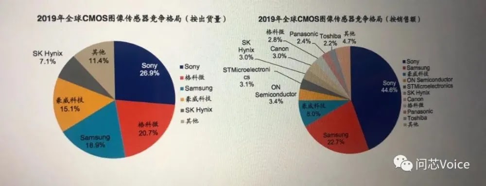
Nikkei Asian Review talks about Samsung and Sony fight for the leadership on the image sensor market:
"Sony, which commands more than half of the market, has prioritized the supply of image sensors to Huawei and other leading smartphone manufacturers. But the strategy has backfired.
"Sony maintains a cautious stance, while Samsung is going on an investment offensive as if now is their chance," said an official with a supplier of equipment used in the production process of image sensors. "The two companies are demonstrating totally different moves."
The comment followed several large orders the supplier won in August and September, all of which were from South Korea's Samsung.
As a late comer to the image sensor market, Samsung has been doing business with Apple and Huawei on a limited scale while attracting smaller customers such as China's Xiaomi and Vivo, which are boosting smartphone production in expectation of demand for alternatives to Huawei versions.
Samsung, therefore, is highly likely to benefit from the rise of smaller Chinese smartphone makers.
Sony, for its part, has a strategy for meeting Samsung's challenge. "We will strive to expand and diversify our customer base looking ahead to fiscal 2021, " Hiroki Totoki, the company's executive deputy president, said at a press conference in October. "Recovery of profitability is expected in earnest in fiscal 2022.", he added.
But one analyst familiar with the matter said it will be difficult for Sony to "fully make up for a drop in supplies to Huawei with an increase in sales to other companies this business year."
"Sony's sensor may not answer the demand needs of (smartphone) makers pursing a high number of pixels," said Tetsuo Omori, senior analyst at Japanese research company Techno Systems Research."
Image Sensors World Go to the original article...
BusinessWire: Velodyne presents a solid-state Veloarray H800:
"The solid state Velarray H800 is architected for automotive grade performance and built using Velodyne’s breakthrough proprietary micro-lidar array architecture (MLA).
...will be available at high-volume production levels with a target price of less than $500 to drive broad adoption in consumer and commercial vehicle markets.
With a field of view of 120 horizontal degrees by 16 vertical degrees, the Velarray H800... provides perception data at a range of up to 200 meters."
Forbes contributor Sabbir Rangwala analyses iPhone 12 LiDAR impact on the market:
"The LiDAR in Apple’s new iPhone moves 3D imaging from the esoteric to the ordinary. It is a significant boost for the technology, similar to photography's transition in the mid-2000s from a specialized world of cameras and lenses to a simple finger-click that can be relished and shared via a general-purpose smartphone by billions of consumers.
Some automotive LiDAR companies are pursuing similar architectures as the iPhone 12 (8XX/9XX nm VCSELs and SPADs). This includes Sense Photonics, Ouster, Opsys Tech, and ZF/Ibeo. Lumentum reportedly supplies VCSELs for the iPhone 12 LiDAR and is also making a focused effort to penetrate the automotive LiDAR market."
CNET quotes iPhone 12 depth accuracy data, as measured by Occipital's VPs of Product Alex Schiff and Anton Yakubenko using their Canvas 3D scanning application:
"The iPhone 12 version of Canvas takes more detailed scans than the first version on the iPad Pro earlier this year, mostly because of iOS 14's deeper access to lidar information, according to Occipital. The newest lidar-enabled version is accurate within a 1% range.
Yakubenko says by Occipital's previous measurements, Apple's iPad Pro lidar offers 574 depth points per frame on a scan, but depth maps can jump up to 256x192 points in iOS 14 for developers. This builds out more detail through AI and camera data."
Fstoppers: DJI adds a LiDAR AF sensor to its RS2 gimbal so that any manual focus lens can be turned into AF one:
Image Sensors World Go to the original article...
SeekingAlpha: Tower Q3 2020 earnings call updates on its image sensor business:
"We have achieved very good results and expect manufacturing to start shortly for lens-type fingerprint sensors. On time-of-flight sensor front, we also received very good results from our lead customer sensors and are moving according to the plan to production in the first half of next year. This would be our first product moving to mass production, using our 300-millimeter stacked wafer backside illumination pixel-level bonding platform.
We continue to see weakness in 2 market segments, the X-ray dental sensor market and the industrial sensor market, however, we begin to see a rebound in customer bond forecast for industrial sensors."
Image Sensors World Go to the original article...
GlobeNewsWire: Himax reports its Q3 results and updates on its image sensor business:
"In smart phone application, Himax targets next generation Android smartphones and the Company is collaborating with leading laser and ToF sensor vendors to develop a new world-facing 3D sensing camera whereby it provides optical components and/or projectors which are critical for the performance of the whole ToF solution.
For non-smartphone 3D-sensing engagements where the Company provides a structured light-based 3D sensing total solution, its target markets range from smart door lock, facial recognition-based e-payment, business access control to biomedical inspection device. A number of recent design-wins will enter into mass production soon.
Alternatively, Himax also offers a market leading 3D decoder ASIC to those customers who wish to design their own structured light 3D sensing solution. Here the Company has had quite a few design-wins from customers targeting China’s vast e-payment market with some shipments already starting in the fourth quarter. The Company is also working with customers for industrial robotics, smart door lock and home security, all of which carry great potential for Himax’s 3D business in the future.
Ultralow power smart sensing
To further lower the technical barrier for using Himax’s WiseEye solution, the Company teamed up with a leading online store specialized in easy development tools for machine learning on edge devices. Himax is extremely excited about the rapid business progress and believes the Company’s WiseEye offerings will become a major contributor to its P&L in the near future.
CMOS Image Sensor
The Company continues to see extremely strong demands for its CMOS image sensors for IP camera and notebook, but its actual shipment has been badly capped by the foundry capacity available to it. Separately, Himax’s industry-first 2-in-1 CMOS image sensor that supports RGB mode for video conferencing and ultralow power AI mode for facial recognition has penetrated the laptop ecosystem for their most stylish super slim bezel designs. The Company expects to have small volume shipment toward late 2020 with more to come in next year.
Regarding ultralow power always-on CMOS image sensor, which targets in battery powered or always-on applications, Himax is getting promising feedback and design adoptions from customers in various markets, such as car recorders, surveillance, smart electric meters, drones, home appliances, and consumer electronics. In Q4, CIS revenue is expected to be flat sequentially although demand is much stronger than that. Again, its shipment is capped by foundry capacity constraint."
Image Sensors World Go to the original article...
BeyonSense-Stratio-LinkSquare demos its SWIR Ge-based sensor capabilities:
Image Sensors World Go to the original article...
Yole Developpement report "Thermal Imagers and Detectors 2020" updates:
"The current surge of EST [elevated body or surface temperature] applications has transformed the thermal imager manufacturer landscape, at least for thermography. In 2019, US and EU players (FLIR, Lynred, SEEK) were leading this market. Enter COVID-19, and Chinese players (Guide IR, Hikvision, Iray) have turned the tables, surpassing the market leaders, at least in shipments. They rapidly addressed the great domestic demand for thermal imaging systems. Having acquired in the past few years technical competences in thermal imager manufacturing, these Chinese players ramped up their domestic production during the last 2 years, and the current situation has fueled their path to becoming stars. As the epidemic spread across geographies to the west, the rest of the companies reaped the benefits from this hype. But western countries were slower in adopting thermal cameras en masse, due to privacy concerns.
In general, thermal imager production lines are not like other integrated circuit (IC) production lines that work at more than 90% of production capacity. Therefore, for some companies there was not a particular need for investment, besides some increase in consumables and possibly workforce. But for some Chinese companies, it is highly possible that the government has supported their production ramp ups. Moreover, this situation could push Chinese companies to chase investments for future growth, which could rapidly develop the market in the future.
But what could happen next year? Chinese manufacturers have enormous production capacity which risks being left unused. We could be spectators to huge changes in strategy where they could:
At this point, many uncertainties exist. One thing is sure: exciting times lie ahead for the thermal imaging industry."
Image Sensors World Go to the original article...
Arxiv.org paper "HDR Imaging with Quanta Image Sensors: Theoretical Limits and Optimal Reconstruction" by Abhiram Gnanasambandam and Stanley H. Chan from Purdue University shows DR advantage of QIS over CIS:
"High dynamic range (HDR) imaging is one of the biggest achievements in modern photography. Traditional solutions to HDR imaging are designed for and applied to CMOS image sensors (CIS). However, the mainstream one-micron CIS cameras today generally have a high read noise and low frame-rate. These, in turn, limit the acquisition speed and quality, making the cameras slow in the HDR mode. In this paper, we propose a new computational photography technique for HDR imaging. Recognizing the limitations of CIS, we use the Quanta Image Sensor (QIS) to trade the spatial-temporal resolution with bit-depth. QIS is a single-photon image sensor that has comparable pixel pitch to CIS but substantially lower dark current and read noise. We provide a complete theoretical characterization of the sensor in the context of HDR imaging, by proving the fundamental limits in the dynamic range that QIS can offer and the trade-offs with noise and speed. In addition, we derive an optimal reconstruction algorithm for single-bit and multi-bit QIS. Our algorithm is theoretically optimal for all linear reconstruction schemes based on exposure bracketing. Experimental results confirm the validity of the theory and algorithm, based on synthetic and real QIS data."
Image Sensors World Go to the original article...
Brookman compares continuous and pulsed iToF approaches with respect to the tolerance to ambient light:
Image Sensors World Go to the original article...
BusinessWire: SmartSens Founder and CEO Richard Xu received a 2020 Innovator of the Year Award at ASPENCORE Global High-Tech Executive Forum.
In an interview with ASPENCORE China analyst, Xu comments on the future of SmartSens:
“As a CMOS image sensor chip design company driven by innovation, SmartSens has selected the technically demanding security product industry as a market entry point. We’ve able to take advantage of the country’s rapid advancements and explosive growth in smart cities and intelligent transportation to become a leader in this field.
In particular, our ultra-starlight-level full-color night vision imaging technology, Stack BSI Global Shutter technology, single-frame HDR technology, and Near-Infrared Enhancement technology among others that have garnered recognitions by leading customers in the security industry.”
Regarding the future of semiconductor industry in China, Xu says:
“Currently, the country can only provide 15% of the overall chip supply, while the demand is over 50%. In addition, there is a demand for high-end chip customization. This presents an opportunity for the domestic semiconductor industry to tap into this rapid development.
From a more passive point of view, it means that domestic companies must examine their own potential. Technological innovation is the key. With a global strategy and strong national sentiment, as well as respect of intellectual property and common-ground value, the market will prove that a win-win situation is attainable.”
Image Sensors World Go to the original article...
BusinessWire: ON Semiconductor introduces a single point dToF LiDAR solution based on the company's Silicon Photomultiplier (SiPM). The SiPM dToF LiDAR Platform can detect objects at distances between 10 cm and 23 m.
The SiPM dToF LiDAR Platform provides a complete solution for low cost, single point LiDAR that OEMs can adapt and take into production to create industrial range finding applications. It includes the NIR laser diode, SiPM sensor and optics, as well as the digital processing necessary to convert the detected signals into elapsed time, and elapsed time into distance.
BusinessWire: Luminar makes a number of public announcements toward closing its reverse merging IPO deal: