Image Sensors World Go to the original article...
SystemPlus publishes a reverse engineering report of poLight AF lens:poLight AF Reverse Engineering
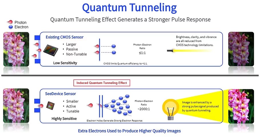
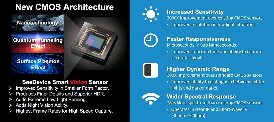
SeeDevice Updates its Comparisons
Image Sensors World Go to the original article...
SeeDevice added few more comparisons of its Quantum Tunneling PAT-PD imager with CMOS sensors:
Michael Tompsett and Bell Labs Receive Emmy Award for the First CCD Imager
Image Sensors World Go to the original article...
Cape Cod Chronicle and Nokia Bell Labs report that The National Academy of Television Arts & Sciences 2020 technical Emmy award winners goes to imaging CCD inventors Michael Tompsett and Bell Labs. Tompsett's invention of CCD imager launched the digital imaging industry and was used in the first commercially available digital cameras.
Huawei Mate 40 Features Always-On Front Camera
Image Sensors World Go to the original article...
Huawei announces its Mate 40 series smartphones with new camera features. The front camera implements an always-on vision-based user interface:
"HUAWEI Mate 40 Pro and HUAWEI Mate 40 Pro+ are set to revolutionise how consumers integrate smartphones into their lives with new user-centric features including Smart Gesture Control, which allows total hands-free control of your device. Simply hover your hand over the device to wake it up or navigate your phone by swiping left, right, up and down. There is also an air press gesture for call answering.
A device that is always there for you, the all new dynamic Eyes on Display on HUAWEI Mate 40 Pro and HUAWEI Mate 40 Pro+ can be activated at a glance, with fully customisable interactive displays hosting all the information you need from your phone. The ring of incoming calls can be reduced by making eye contact with your phone."
Here are official Huawei demos of its low-power vision camera:
Smartsens Raises $225M
Image Sensors World Go to the original article...
OTCbeta, DoNews: Smartsens receives a new investment from China National Integrated Circuit Industry Big Fund Phase II, Xiaomi Yangtze River Industry Fund, and Anxin Investment. This follows an early August 2020 investment from Hubble Investment fund under Huawei.
Update: DealStreetAsia reports that the new investment is approximately 1.5b RMB (about $225M).
Paper on CG Improvements
Image Sensors World Go to the original article...
Assim Boukhayma (Senbiosys & EPFL) publishes an Arxiv.org paper "Conversion Gain Enhancement in Standard CMOS Image Sensors."
"This paper focuses on the conversion gain (CG) of pixels implementing pinned photo-diodes (PPD) and in-pixel voltage follower in standard CMOS image sensor (CIS) process. An overview of the CG expression and its impact on the noise performance of the CIS readout chain is presented. CG enhancement techniques involving process refinements and pure circuit design and pixel scheme optimization are introduced. The implementation of these techniques in a 180 nm CIS process demonstrates a progressive enhancement of the CG by more than a factor 3 with respect to a standard reference pixel from the same foundry, allowing a better understanding of the different parasitic elements on the sense node capacitance and CG."
Nanorod-based CMY CFA
Image Sensors World Go to the original article...
Arxiv.org paper "A new CMY camera technology using Al-TiO2-Al nanorod filter mosaic integrated on a CMOS image sensor" by Xin He, Y. Liu, P. Beckett, H. Uddin, A. Nirmalathas, and R. R. Unnithan from e University of Melbourne, RMIT University, and Australian National Fabrication Facility proposes to revive complementary color CFAs:
"A CMY colour camera differs from its RGB counterpart in that it employs a subtractive colour space of cyan, magenta and yellow. CMY cameras tend to performs better than RGB cameras in low light conditions due to their much higher transmittance. However, conventional CMY colour filter technology made of pigments and dyes are limited in performance for the next generation image sensors with submicron pixel sizes. These conventional filters are difficult to fabricate at nanoscale dimensions as they use their absorption properties to subtract colours. This paper presents a CMOS compatible nanoscale thick CMY colour mosaic made of Al-TiO2-Al nanorods forming an array 0.82 million colour pixels of 4.4 micron each, arranged in a CMYM pattern. The colour mosaic was then integrated onto a MT9P031 monochrome image sensor to make a CMY camera and the colour imaging demonstrated using a 12 colour Macbeth chart. The developed technology will have applications in astronomy, low exposure time imaging in biology and photography."
Yole on LiDAR Market: Prices Drop but Volume Does Not Grow
Image Sensors World Go to the original article...
EETimes publishes Yole Developpement interview on LiDAR Market:
"Historically, LiDAR systems have been too expensive to mass-produce for consumer vehicles. The trend is now reversing: Different LiDAR manufacturers have defined aggressive strategies, and the price drop over the past three years has been massive.
Last year, Luminar announced LiDAR-based solutions for under US$1,000. Velodyne, which came up with the first real-time 3D LiDAR in 2005, unveiled plans to reach an average unit price of US$600 by 2024, down from US$17,900 in 2017. And Chinese LiDAR manufacturers, whose unit prices are usually one-fifth those of other companies, are already fielding units priced below $1,000 and are gaining market share.
But a price drop does not necessarily imply a volume increase. So far, volumes have not grown significantly, and mass adoption has not yet occurred. “LiDAR must answer a need,” said Debray. “In the industrial market, including manufacturing and logistics, there is a clear trend toward automation, and LiDAR is playing a key role. In automotive, US$600 remains expensive for a car sensor in comparison with ADAS cameras, for which the average selling price is US$80. Therefore, we are now hearing about US$100 LiDAR for short-range automotive applications.”
Smartsens 2.7um Pixel Combines Global Shutter with 40% QE @ 940nm
Image Sensors World Go to the original article...
Smartsens unveils a 1.3MP pixel global shutter image sensor SC133GS. The new sensor uses 2.7μm pixels in 1/4" optical format and is aimed to the DMS systems to monitor the driver's driving state and attention to driving safety.PCO Explains its Image Intensified Cameras
Tip Avalanche Photodiode Claimed to Overcome SPAD Limitations
Image Sensors World Go to the original article...
Arxiv.org paper "Tip Avalanche Photodiode -- A new generation Silicon Photomultiplier based on non-planar technology" by Eugen Engelmann, Wolfgang Schmailzl, Peter Iskra, Florian Wiest, Elena Popova, and Sergey Vinogradov from KETEK, Germany, and MEPhI, Russia, promises to revolutionize SPAD design:SystemPlus Reverse Engineers Tesla 3 Tri-Camera
Image Sensors World Go to the original article...
Yole Developpement publishes a webinar "From Advanced Driver-Assistance Systems (ADAS) to Automated Driving" with a part discussion Tesla 3 Tri-camera:Unispectral Presents its Tunable MEMS Filter for Multispectral Imaging
Image Sensors World Go to the original article...
Unispectral CTO Peleg Levin presents his company's approach to multispectral imaging:
Canon Announces Several Sensors
Image Sensors World Go to the original article...
Canon, Canon: Canon announces two 35mm full-frame CMOS sensors based on the NIR sensitivity improved 19um pixel - the LI3030SAM (monochrome) and LI3030SAI (color/near-NIR)—which feature 3x and 2.3x enhanced NIR sensitivity respectively (at 800nm) compared to the predecessor products.
The LI3030SAM is said to be capable of monochrome video capture in low-light environments with as little as 0.0005 lux of illumination.
Apparently, the same sensors have been presented as in-development projects a couple of months ago.
Canon: Another announcement is 250MP 5fps APS-H sensors with 1.5um pixel, the LI8020SAC (color) and LI8020SAM (monochrome). They look fairly similar to a sensor first unveiled 5 years ago and re-announced several times since then.
Canon: Another sensor is 2.12MP LI7050SAC for security cameras "featuring a pixel pitch of 4.1 μm and a resolution of approximately 2.12 million pixels, the sensor provides a High Dynamic Range (HDR) of equivalent to up to 20 stops with frame rates of 30fps and 60fps. What’s more, the sensor features a 54,000 green sensitivity level and can read 1936 × 1096 pixels, which is slightly higher than HD resolution." That one appears to be announced for the fist time.
Atomic Layer Deposition for Image Sensors
Image Sensors World Go to the original article...
Mikko Söderlund of Beneq presents Atomic Layer Deposition for image sensors to achieve:
- barrier coating
- surface passivation
- anti-reflection coating
ON Semi Expands 3.2um Global Shutter Sensor Family
Image Sensors World Go to the original article...
BusinessWire: ON Semiconductor expands its XGS family of image sensors with low noise products that combine 12-bit image at a high frame rate. The new offerings include the XGS 45000, the XGS 30000, and the XGS 20000 with up to 45 MP resolution and up to 60 fps in 8K video mode. Also available is the new XGS 5000 with low power performance for compact 29 x 29 mm2 camera designs. Alongside the XGS 5000, 3 MP and 2 MP variants have been released for production.
All XGS devices feature a 3.2 μm pixel and aim to IoT applications such as machine vision and Intelligent Transportation Systems (ITS).
Light Field Camera for Smartphone
Image Sensors World Go to the original article...
MDPI paper "Miniaturized 3D Depth Sensing-Based Smartphone Light Field Camera" by Hyun Myung Kim, Min Seok Kim, Gil Ju Lee, Hyuk Jae Jang, and Young Min Song from Gwangju Institute of Science and Technology, Korea, proposes a simplified approach for lightfield imaging:
"The miniaturization of 3D depth camera systems to reduce cost and power consumption is essential for their application in electrical devices that are trending toward smaller sizes (such as smartphones and unmanned aerial systems) and in other applications that cannot be realized via conventional approaches. Currently, equipment exists for a wide range of depth-sensing devices, including stereo vision, structured light, and time-of-flight. This paper reports on a miniaturized 3D depth camera based on a light field camera (LFC) configured with a single aperture and a micro-lens array (MLA). The single aperture and each micro-lens of the MLA serve as multi-camera systems for 3D surface imaging. To overcome the optical alignment challenge in the miniaturized LFC system, the MLA was designed to focus by attaching it to an image sensor. Theoretical analysis of the optical parameters was performed using optical simulation based on Monte Carlo ray tracing to find the valid optical parameters for miniaturized 3D camera systems. Moreover, we demonstrated multi-viewpoint image acquisition via a miniaturized 3D camera module integrated into a smartphone."
Yole Forum on Machine Vision and Thermal Cameras 2020: Prices Go Down, Resolutions Go Up
Image Sensors World Go to the original article...
Yole Developpement kindly allowed me to publish few slides from its "Machine Vision & IR for Industry Forum 2020" held in Shenzhen, China, on Sept. 11:
Galaxy Note 20 Ultra Uses ST AF Sensor instead of Sony iToF
Image Sensors World Go to the original article...
TechInsights teardown reveals that Samsung Galaxy Note 20 Ultra uses ST AF sensor instead of Sony Sony IMX516 iToF in the previous generation:Camera Array for Multi-Spectral Imaging
Image Sensors World Go to the original article...
IEEE Transactions on Image Processing publishes a paper "Camera Array for Multi-Spectral Imaging" by Nils Genser, Jürgen Seiler, and André Kaup from Friedrich-Alexander-Universität Erlangen-Nürnberg (FAU), Germany, that might justify even more cameras in smartphones than it's used now.
"Recently, many new applications arose for multi-spectral and hyper-spectral imaging. Besides modern biometric systems for identity verification, also agricultural and medical applications came up, which measure the health condition of plants and humans. Despite the growing demand, the acquisition of multi-spectral data is up to the present complicated. Often, expensive, inflexible, or low resolution acquisition setups are only obtainable for specific professional applications. To overcome these limitations, a novel camera array for multi-spectral imaging is presented in this article for generating consistent multi-spectral videos. As differing spectral images are acquired at various viewpoints, a geometrically constrained multi-camera sensor layout is introduced, which enables the formulation of novel registration and reconstruction algorithms to globally set up robust models. On average, the novel acquisition approach achieves a gain of 2.5 dB PSNR compared to recently published multi-spectral filter array imaging systems. At the same time, the proposed acquisition system ensures not only a superior spatial, but also a high spectral, and temporal resolution, while filters are flexibly exchangeable by the user depending on the application. Moreover, depth information is generated, so that 3D imaging applications, e.g., for augmented or virtual reality, become possible. The proposed camera array for multi-spectral imaging can be set up using off-the-shelf hardware, which allows for a compact design and employment in, e.g., mobile devices or drones, while being cost-effective."
Forza Webinar on Image Sensor Interfaces
Image Sensors World Go to the original article...
Forza publishes its webinar "CMOS Image Sensor Signal Interface & Lessons Learned From System Prototyping" by Nguyen Tran:
Sony Talks about Intelligent Sensors and their Use Cases
Image Sensors World Go to the original article...
Sony publishes a video promoting its sensors with integrated AI processor:GPixel APS-C Global Shutter Sensor Combines 21MP Resolution with 1,000 fps Speed
Image Sensors World Go to the original article...
Gpixel announces a high-speed global shutter image sensor, GSPRINT4521, the first in a new family of products targeting high speed applications.
GSPRINT4521 is a 21MP (5120 x 4096) APS-C sized (29.5mm) sensor with 4.5μm charge domain global shutter pixel. It achieves more than 35ke– FWC and less than 3e– rms read noise, resulting in an intra-scene DR of up to 69 dB in single gain operation and up to 81 dB in dual gain HDR mode.
GSPRINT4521 will be offered in different speed variants. The full speed version of the sensor consists of 160 pairs of sub-LVDS channels running at 1.2Gbps each, which delivers a 1000 fps at full resolution in 8-bit mode, 500 fps in 10-bit mode, and 250 fps in 12-bit mode in single gain operation. ROI and on-chip binning modes can be used to further increase the frame rates. Lower frame rates are enabled by multiplexing to a reduced number of output channels (down to 4 channels). A reduced speed version of the sensor, optimized for 50 Gbps camera interfaces, will also be available. GSPRINT4521 is packaged in a 454-pin uPGA ceramic package and will be available in both monochrome and color.
“With the launch of the first sensor in the GSPRINT family, Gpixel is able to address a new segment of applications requiring higher frame rates and/or high dynamic range, low noise global shutter operation. We are excited to offer our technology to support these demanding applications and are very much looking forward to the further expansion of this new series,” says Wim Wuyts, CCO of Gpixel.
High frame rate, generous pixel size and low read noise make GSPRINT4521 an ideal solution for applications such as high-speed 4K video, industrial inspection, motion analysis and life science imaging.
GSPRINT4521 monochrome engineering samples can be ordered today for delivery in November 2020.
Apple Unveils 2 iPhones with LiDAR
Image Sensors World Go to the original article...
Apple new iPhone 12 Pro and iPhone 12 Pro Max feature LiDARs integrated in the rear camera cluster. Among other things, the LiDAR is promised to improve AF speed by 6x in low light: