CP+ 2022 On-site Event at Pacifico Yokohama Canceled
Canon requests removal of toner cartridges offered by zhu hai chuang yue xin ke ji you xian gong si via Amazon
Canon’s activities lead to the removal of 2,224 listings from Amazon in Germany, Italy, Spain, the United Kingdom, France, The Netherlands and Turkey
57 listings removed from Amazon in Canada, Mexico and the United States of America after Canon files infringement reports
Thesis on Current-Assisted SPAD Sensors
Image Sensors World Go to the original article...
Vrije Universiteit Brussel publishes a PhD thesis "Current-assisted SPAD sensors fabricated in conventional CMOS process" by Gobinath Jegannathan.
"In this work, a novel SPAD sensor is presented where the novelty arises from the integration of a large absorption volume and a very small avalanche multiplication volume. Such a detector topology allows to have a thick absorption layer which leads to higher quantum efficiencies for NIR wavelengths. This integration is enabled by “current-assistance” principle where a drift field is created in the substrate by applying a potential gradient. This “current-assisted SPAD” is fabricated in a cost-effective CMOS process which is commercially available."


trinamiX Face Authentication is the First to be Certified as Highly secure Behind OLED
Image Sensors World Go to the original article...
trinamiX Face Authentication is the world’s first to fulfill highest biometric security demands while the hardware is invisibly mounted behind an OLED display. The solution was lately put to the thorough test of accredited assessment institutes. It was certified to be spoof-proof behind OLED according to the top standards defined by Android and FIDO Alliance.
To give proof of its higher security, trinamiX has put their technology to the test of accredited assessment institutes. Over a period of several months, it has undergone thousands of spoof attempts including the use of silicone masks with accurate three-dimensional shape. As a result, their face authentication solution has successfully been certified as spoof-proof (Spoof Acceptance Rate = 0 %) according to Android Biometric Class 3 (strong). It furthermore showed to fulfill the high requirements of FIDO Level C – the alliance’s soon-to-be top standard. Based on these assessments, trinamiX Face Authentication is officially approved for integration into Android phones as well as for use in sensitive applications like mobile payment. As the world’s first face authentication solution, it passed all biometric security tests while the hardware was mounted behind an OLED display.
Startups Funding in January 2022
Image Sensors World Go to the original article...
Semiconductor Engineering publishes "Startup Funding: January 2022" There is a number of imaging startups in the list, mostly from China:- Keyang Semiconductor (KYS) raised over CNY 100.0M (~$15.8M) in a strategic investment. The company offers packaging and testing services, with a focus on wafer-level packaging, TSV packages, and fingerprint recognition devices. The funds will be used to upgrade its CIS production line. Founded in 2013, it is based in Suzhou, China.
- Hefei Sensor Turnkey Service (HSTS) raised nearly CNY 50.0M (~$7.9M) in a Series A round that included Hefei Industry Investment Group. HSTS specializes in CIS packaging and testing services covering 8-inch and 12-inch wafer testing, grinding, cutting, and module and terminal IC testing. Funds will be used to purchase equipment and in development of new production lines. Founded in 2020, it is based in Hefei, China.
- Silicon Integrated raised “several hundred million yuan” (CNY 100.0M is ~$15.8M) in Series D financing led by Wuyuan Capital, joined by ByteDance, Juhua Chuanxin Investment, and existing shareholders including Huaye Tiancheng and Source Code Capital. Silicon Integrated line of ToF 3D sensors uses BSI process with applications in face identification, AR/VR, motion capture, 3D modeling, machine vision, and automotive. It is also investing in color temperature detection for OLED screens, multispectral sensing, and ranging. Funds will be used for further iteration and commercialization of existing product lines, expanding to new products, and hiring. Founded in 2016, it is based in Wuhan, China.
- GWIC, also known as North GuangWei, raised an undisclosed amount in strategic financing from Fujirui Optoelectronics. GWIC produces uncooled infrared detectors for military, automotive, security, and other night vision applications. Founded in 2006, it is based in Beijing, China.
- Mojo Vision raised $45.0M in Series B financing from Amazon Alexa Fund, PTC, Edge Investments, HiJoJo Partners, and others. Existing investors New Enterprise Associates, Liberty Global Ventures, Advantech Capital, AME Cloud Ventures, Dolby Family Ventures, Motorola Solutions Venture Capital, and Open Field Capital also participated. Mojo Vision’s contact lens uses a self-designed low power image sensor. The company is currently working on FDA approval. A particular focus for the company is providing performance data and real-time stats to athletes, and it has partnered with several sports apparel and app brands. Founded in 2015, it is based in Saratoga, California, USA.
- Owl Autonomous Imaging drew $15.0M in Series A funding. OwlAI offers a monocular 3D thermal imaging and ranging solutions for automotive active safety systems. The company says the system is particularly good at detecting pedestrians and cyclists more quickly than other sensor types and works in poor lighting and weather conditions. Founded in 2018, it is based in Fairport, New York, USA.
- Lidar developer RoboSense received an undisclosed amount in strategic investment from EV company BYD. RoboSense is aiming to go public in Hong Kong later this year. Founded in 2014, it is based in Shenzhen, China.
- VisionICs Microelectronics raised “hundreds of millions of yuan” (CNY 100.0M is ~$15.8M) in strategic financing from Chendao Capital, GoerTek, BYD, and others. The startup develops SPAD dToF sensors, with products including both 1D dToF and 3D dToF chips. Applications include robotic vacuum cleaners, UAVs, and mobile phones, as well as AR/VR, smart home, and automotive lidar. Funding will be used for mass production and developing new products. Founded in 2018, it is based in Nanjing, China.
- Automotive lidar startup Zvision Technologies, also known as Yijing Technology, raised “hundreds of millions of yuan” (CNY 100.0M is ~$15.8M) in pre-Series C funding from Xpeng Motors, Shang Qi Capital, Dongfeng Asset Management, and Intel Capital. The startup develops solid state MEMS lidar systems with long-range and short-range options. Funds will be used for R&D and to move to mass production. Based in Beijing, China, the company was founded in 2017.
Sony Reports Quarterly Results
Image Sensors World Go to the original article...
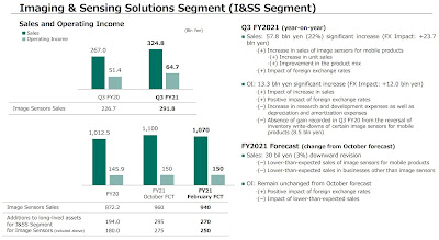
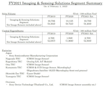
Sony reports its quarterly results for the quarter ended on January 31, 2021:
- Despite severe conditions in the smartphone market, such as weakness in the Chinese market and shortages of components, especially semiconductors, the efforts we have made heretofore to expand and diversify our mobile sensor customer base, as well as to recover our market share on a volume basis, are having some success.
- However, it is taking longer than expected to introduce the high-performance, high resolution custom sensors that we have been working on with Chinese smartphone makers, so the speed of profitability improvement resulting from an increase in addedvalue products going into next fiscal year will be slightly lower than originally planned.
- Recently, the trend toward Chinese smartphone makers purchasing larger-sized sensors for their high-end products is improving after having stagnated due to the contraction of our business with a certain Chinese customer. We expect the Chinese smartphone market to normalize in the second half of next fiscal year.
- Since we feel better about the possibility of sales growth and further market share expansion next fiscal year, we will focus even more on increasing the added-value of our products and strive to improve profitability.
- On January 25, 2022, Sony Semiconductor Solutions Corporation completed its initial investment in Japan Advanced Semiconductor Manufacturing Co., Ltd. (“JASM”), as a minority shareholder.
- Sony will support JASM by assisting with the start-up of this new logic wafer factory which aims to begin mass production during calendar year 2024.
IC Insights: CIS Sales Did Not "Surge" in 2021
Image Sensors World Go to the original article...
IC Insights market report says that "Optoelectronics sales growth was muted in the 2021 rebound due to the lack of a surge in CMOS image sensors, which were held back by trade frictions and technology disputes between the U.S. and China, fluctuations in some key end-use applications, and shortages of ICs and other components used in digital-imaging systems. Optoelectronics sales increased 9% in 2021 to a record-high $47.9 billion, and the large CMOS image sensor category only grew 6% to $20.3 billion last year, says the January report."Olympus CAMEDIA C-2000 Z retro review
Superlattice-based Imagers
Image Sensors World Go to the original article...
Center for Quantum Devices at Northwestern University publishes a presentation on superlattices for low noise imaging from UV to VLWIR by Manijeh Razeghi:
MIPI Adopts A-PHY v1.1
Image Sensors World Go to the original article...
MIPI Alliance adopts A-PHY v1.1 automotive SerDes, doubling the maximum downlink data rate from 16 Gbps to 32 Gbps, doubling the uplink data rate and providing manufacturers with additional implementation options.


Silkworms Create Image Sensor-based Security Device
Image Sensors World Go to the original article...
PRNewswire: A physical unclonable function (PUF) is a physical feature that takes advantage of microscopic differences in electronics to create unique security "keys." These keys, when read by an electronic device, help establish or refute the authenticity of the input, thereby either granting or denying access. Now, researchers from the Gwangju Institute of Science and Technology, Korea, have designed the first natural PUF. Using native silk fibers obtained from Bombyx mori (domesticated silkworms), the research team designed PUF-based tags. These tags were then used to devise a lens-free, optical (light-based), and portable PUF (LOP-PUF) module.
Silkworms Create Image Sensor-based Security Device
Image Sensors World Go to the original article...
PRNewswire: A physical unclonable function (PUF) is a physical feature that takes advantage of microscopic differences in electronics to create unique security "keys." These keys, when read by an electronic device, help establish or refute the authenticity of the input, thereby either granting or denying access. Now, researchers from the Gwangju Institute of Science and Technology, Korea, have designed the first natural PUF. Using native silk fibers obtained from Bombyx mori (domesticated silkworms), the research team designed PUF-based tags. These tags were then used to devise a lens-free, optical (light-based), and portable PUF (LOP-PUF) module.Canon aids relief effort following volcano eruption and tsunami in the Kingdom of Tonga
Hynix Begins Mass Production of 0.7um Pixels
Image Sensors World Go to the original article...
BusinessKorea: Keeping an earlier promise, SK Hynix has started to mass-production of 50MP sensors with 0.7㎛ pixels. The image quality is said to be "at the same level as Sony products."Chinese CIS Companies Report All-Time High Profits
Image Sensors World Go to the original article...
SecuritiesTimes: Omnivision's net profit in 2021 is expected to be in range of 4.468 billion to 4.868 billion yuan, a year-on-year increase of 65.13% to 79.91%. The net profit after deducting "non-deductible items" (?) is 3.918 billion to 4.268 billion yuan, a year-on-year increase of 74.51% to 90.10%.
Galaxycore too expects operating income of 6.652 billion to 7.492 billion yuan in 2021, net profit of 1.135 billion to 1.35 billion yuan, a year-on-year increase of 46.83% to 74.57%; Profits ranged from 1.086 billion to 1.291 billion yuan, a year-on-year increase of 41.75% to 68.52%, both of which are expected to exceed the revenue growth rate over the same period.
Indeed, Strategy Analytics reports show that Omnivision and other Chinese companies increase their smartphone market share at the expense of Sony and Samsung:


Canon requests removal of toner cartridges offered by xianshi yanliangqucanranbaihuoshanghang via Amazon
Panasonic Develops Low-Cost LWIR Lens
Image Sensors World Go to the original article...
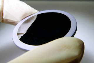
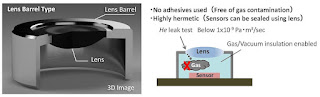
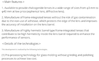
Panasonic has developed a mass production technology of low-cost far-IR aspherical lenses. These lenses are made of chalcogenide glass having excellent transmission characteristics in the far-IR. In addition to realizing low-cost (approx. half compared to the company’s conventional method) by newly developed glass molding method and mold processing technology, Panasonic is now able to offer a variety of lenses such as diffractive lens, the world's first* highly hermetic frame-integrated lens without using adhesive (leak detection accuracy of less than 1x10⁻⁹ Pa・m3/sec in helium leak test).
A low-cost silicon that has been commonly used as the lens material for far-IR sensors is not suitable for high pixel counts due to its low transmittance, so germanium spherical lenses having high transmittance are widely used as the number of pixels increases. However, as the pixel count increases further, the effect of aberration caused by a spherical lens becomes more pronounced. To reduce this effect, combination of many spherical lenses and an aspherical lens will be required, which leads to increase in cost and size.
To resolve this problem, Panasonic has developed a new technology for the low-cost production of high-performance aspherical lenses suitable for far-infrared optical systems, based on the glass molding technology the company cultivated through the production of visible light aspherical lenses for cameras.
Hermetic sealing is important for thermal imaging camera modules. A low cost lens solution makes thermal cameras more accessible to general consumer applications.
SmartSens News
Image Sensors World Go to the original article...
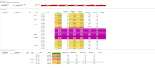
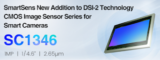
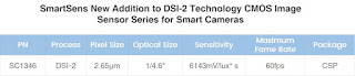
PRNewswire: PDF Solutions announces that SmartSen has selected Exensio Fabless as the platform to perform data management and analytics for their entire family of CIS products.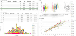




Recent Videos: CEA-Leti, Himax, Gigajot, Trieye, Pixart, Oculi
Image Sensors World Go to the original article...
CEA-Leti publishes a video about its low power always-on image sensor presented in May last year:



ESPROS Presents OHC15L Process
Image Sensors World Go to the original article...
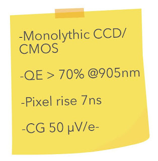
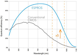
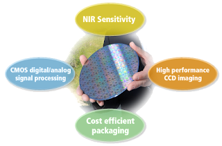
Espros presents its new CCD-CMOS process OHC15L: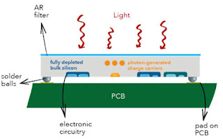
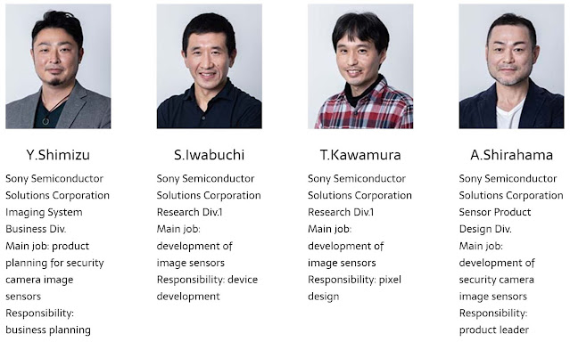
Interview with Sony STARVIS 2 Designers
Image Sensors World Go to the original article...
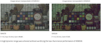
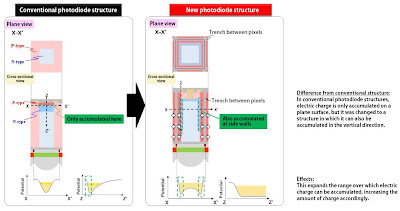
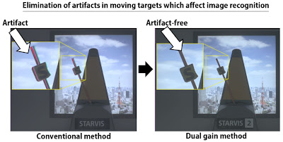
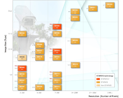
In June 2021, Sony introduced STARVIS 2 pixel technology for security cameras: