How to backup photos
CFP: International Workshop on Image Sensors and Imaging Systems 2022
Image Sensors World Go to the original article...
The 5th International Workshop on Image Sensors and Imaging Systems (IWISS2022) will be held in December 2022 in Japan. This workshop is co-sponsored by IISS.
-Frontiers in image sensors based on conceptual breakthroughs inspired by applications-
Date: December 12 (Mon) and 13 (Tue), 2022
Venue: Sanaru Hall, Hamamatsu Campus, Shizuoka University
Access: see https://www.eng.shizuoka.ac.jp/en_other/access/
Address: 3-5-1 Johoku, Nakaku, Hamamatsu, 432-8561 JAPAN
Official language: English
Overview
In this workshop, people from various research fields, such as image sensing, imaging systems, optics, photonics, computer vision, and computational photography/imaging, come together to discuss the future and frontiers of image sensor technologies in order to explore the continuous progress and diversity in image sensors engineering and state-of-the-art and emerging imaging systems technologies. The workshop is composed of invited talks and a poster session. We are accepting approximately 20 poster papers, whose submission starts in August, with deadline on October 14 (Fri), 2022. A Poster Presentation Award will be given to the selected excellent paper. We encourage everyone to submit the latest original work. Every participant is required to register online by December 5 (Mon), 2022. On-site registration is NOT accepted. Since the workshop is operated by a limited number of volunteers, we can offer only minimal service; therefore, no invitation letters for visa applications to enter Japan can be issued.
Latest Information: Call for Paper, Advance Program
http://www.i-photonics.jp/meetings.html#20221212IWISS
Poster Session
Submit a paper: https://www.ite.or.jp/ken/form/index.php?tgs_regid=faf9bc5bde5e430962d98b110ccac65c5ddc6ca5718edb7c80089461c48b9cfa&tgid=ITE-IST&lang=eng&now=20220719133618
Submission deadline: Oct. 14(Fri), 2022 (Only title, authors, and short abstract are required)
Please use the above English page. DO NOT follow the Japanese instructions at the bottom of the page.
Notification of acceptance: by Oct. 21 (Fri)
Manuscript submission deadline: Nov. 21 (Mon), 2022 (2-page English proceeding is required)
One excellent poster will be awarded.
Plenary and Invited Speakers
[Plenary]
“Deep sensing - Jointly optimize imaging and processing –“ by
Hajime Nagahara (Osaka University, Japan)
[Invited Talks]
- Image Sensors
“InGaAs/InP and Ge-on-Si SPADs for SWIR applications” by Alberto Tosi (Politecnico di Milano, Italy)
“CMOS SPAD-Based LiDAR Sensors with Zoom Histogramming TDC Architectures” by Seong-Jin Kim et al. (UNIST, Korea)
"TBD" by Min-Sun Keel (Samsung Electronics, Korea)
“Modeling and verification of a photon-counting LiDAR” by Sheng-Di Lin (National Yang Ming Chiao Tung Univ., Taiwan)
- Computational Photography/Imaging and applications “Computational lensless imaging by coded optics” by Tomoya Nakamura (Osaka Univ., Japan)
“TBD” by Miguel H. Conde (Siegen Univ.) “TBD” by TBD (Toronto Univ.)
- Optics and Photonics
“Optical system integrated time-of-flight and optical coherence tomography for high-dynamic range distance measurement” by Yoshio Hayasaki et al. (Utsunomiya Univ., Japan)
“High-speed/ultrafast holographic imaging using an image sensor” by Yasuhiro Awatsuji et al. (Kyoto Institute of Technology, Japan)
“Near-infrared sensitivity improvement by plasmonic diffraction technology” by Nobukazu Teranishi et al. (Shizuoka Univ, Japan)
Scope
- Image sensor technologies: fabrication process, circuitry, architectures
- Imaging systems and image sensor applications
- Optics and photonics: nanophotonics, plasmonics, microscopy, spectroscopy
- Computational photography/ imaging
- Applications and related topics on image sensors and imaging systems: e.g., multi-spectral imaging, ultrafast imaging, biomedical imaging, IoT, VR/AR, deep learning, ...
Online Registration for Audience
Registration is necessary due to the limited number of available seats.
Registration deadline is Dec. 5 (Mon).
Register and pay online from the following website: <to appear>
Registration Fee
Regular and student: approximately 2,000-yen (~15 USD)
Note: This price is for purchasing the online proceeding of IWISS2022 through the ITE. If you cannot join the workshop due to any reason, no refund will be provided.
Collaboration with MDPI Sensors Special Issue
Special Issue on "Recent Advances in CMOS Image Sensor"
Special issue editor: Dr. De Xing Lioe
Paper submission deadline: Feb. 25 (Sat), 2023
https://www.mdpi.com/journal/sensors/special_issues/CMOS_image_sensor
The poster presenters are encouraged to submit a paper to this special issue!
Note-1: Those who do not give a presentation in the IWISS2022 poster session are also welcome to submit a paper!
Note-2: Sensors is an open access journal, the article processing charges (APC) will be applied to accepted papers.
Note-3: For poster presenters of IWISS2022, please satisfy the following conditions.
The submitted extended papers to the special issue should have more than 50% new data and/or extended content to make it a real and complete journal paper. It will be much better if the Title and Abstract are different with that of conference paper so that they can be differentiated in various databases. Authors are asked to disclose that it is conference paper in their cover letter and include a statement on what has been changed compared to the original conference paper.
Sponsored by Technical Group on Information Sensing Technologies (IST),
the Institute of Image Information and Television Engineers (ITE)
Co-sponsored by International Image Sensor Society (IISS), Group of
Information Photonics (IPG) +CMOS Working Group, the Optical Society of
Japan, and innovative Photonics Evolution Research Center (iPERC)
[General Chair] Keiichiro Kagawa (Shizuoka Univ., Japan)
[Technical Program Committee (alphabetical order)]
Chih-Cheng Hsieh (National Tsing Hua Univ., Taiwan)
Keiichiro Kagawa (Shizuoka Univ., Japan)
Takashi Komuro (Saitama Univ., Japan)
De Xing Lioe (Shizuoka Univ., Japan)
Hajime Nagahara (Osaka Univ., Japan)
Atushi Ono (Shizuoka Univ., Japan)
Min-Woong Seo (Samsung Electronics, Korea)
Hiroyuki Suzuki (Gunma Univ., Japan)
Hisayuki Taruki (Toshiba Electronic Devices & Storage Corporation, Japan)
Franco Zappa (Politecnico di Milano, Italy)
Contact for any question about IWISS2022
E-mail: iwiss2022@idl.rie.shizuoka.ac.jp
(Keiichiro Kagawa, Shizuoka Univ., Japan)
Nikon 500mm f5.6E PF VR review
Sigma Foveon sensor will be ready in 2022
Image Sensors World Go to the original article...
From PetaPixel:Sigma’s CEO Kazuto Yamaki has revealed that the company’s efforts in making a full-frame Foveon sensor are on track to be finished by the end of the year.

Sigma’s Foveon sensors use a proprietary three-layer structure in which red, green, and blue pixels each have their own full layer. In traditional sensors, the three pixels share a single layer in a mosaic arrangement and the camera “fills in” missing colors by examining neighboring pixels.Since each pixel of a photo is recorded in three colors, the resulting photo should be sharper with better color accuracy and fewer artifacts.
The release had been delayed on at least two occasions in the past due to technical challenges, once in 2020 and again in 2021. The initial announcement about this sensor was made back in 2018. In February 2022, Yamaki indicated that the company was in stage 2 of testing, and the final third stage will involve mass-production testing.
Canon’s activities lead to the removal of 956 listings from Amazon in Germany, Italy, Spain, the United Kingdom, France and The Netherlands
46 listings removed from Amazon in Canada, Mexico and the United States of America after Canon files infringement reports
Viltrox AF 24mm f1.8 review
Prophesee interview in EETimes
Image Sensors World Go to the original article...
EETimes has published an interview with CEO of Prophesee about their event sensor technology. Some excerpts below.

Meaning of "neuromorphic"
Most companies doing neuromorphic sensing and computing have a similar vision in mind, but implementations and strategies will be different based on varying product, market, and investment constraints. ...
... there is a fundamental belief that the biological model has superior characteristics compared to the conventional ...
Markets targeted
... the sector closest to commercial adoption of this technology is industrial machine vision. ...
The second key market for the IMX 636 is consumer technologies, ... the event–based camera is used alongside a full–frame camera, detecting motion ... correct any blur.
Prophesee is also working with a customer on automotive driver monitoring solutions... Applications here include eye blinking detection, tracking or face tracking, and micro–expression detection.
Commercialization strategy
The company recently released a new evaluation kit (EVK4) for the IMX 636. Metavision (simulator) SDK for event–based vision has also recently been open–sourced ...
Future Directions
Prophesee plans to continue development of both hardware and software, alongside new evaluation kits, development kits, and reference designs.
Two future directions...
further reduction of pixel size (pixel pitch) and overall reduction of the sensor to make it suitable for compact consumer applications such as wearables.
... facilitating the integration of event–based sensing with conventional SoC platforms.
“The closer you get to the acquisition of the information, the better off you are in terms of efficiency and low latency. You also avoid the need to encode and transmit the data. So this is something that we are pursuing.”
“The ultimate goal of neuromorphic technology is to have both the sensing and processing neuromorphic or event–based, but we are not yet there in terms of maturity of this type of solution,”
Full article here: https://www.eetimes.com/neuromorphic-sensing-coming-soon-to-consumer-products/?
3D cameras for metaverse
Image Sensors World Go to the original article...
Press release from II-VI Inc. announces joint effort with Artilux on a SWIR 3D camera for the "metaverse".

PITTSBURGH and HSINCHU, TAIWAN, July 18, 2022 (GLOBE NEWSWIRE) – II‐VI Incorporated (Nasdaq: IIVI), a leader in semiconductor lasers, and Artilux, a leader in germanium silicon (GeSi) photonics and CMOS SWIR sensing technology, today announced a joint demonstration of a next-generation 3D camera with much longer range and higher image resolution to greatly enhance user experience in the metaverse.
Investments in the metaverse infrastructure are accelerating and driving the demand for sensors that enable more realistic and immersive virtual experiences. II-VI and Artilux combined their proprietary technologies in indium phosphide (InP) semiconductor lasers and GeSi sensor arrays, respectively, to demonstrate a miniature 3D camera that operates in the short-wavelength infrared (SWIR), at 1380 nm, resulting in significantly higher performance than existing cameras operating at 940 nm.
“The longer infrared wavelength provides better contrasts and reveals material details that are otherwise not visible with shorter-wavelength illumination, especially in outdoor environments,” said Dr. Julie Sheridan Eng, Sr. Vice President, Optoelectronic Devices & Modules Business Unit, II-VI. “By designing a camera that operates at 1380 nm instead of 940 nm, we can illuminate the scene with greater brightness and still remain well within the margins of eye safety requirements. In addition, the atmosphere absorbs more sunlight at 1380 nm than at 940 nm, which reduces background light interference, greatly improving the signal-to-noise ratio and enabling cameras with longer range and better image resolution.”
“The miniature SWIR 3D camera can be seamlessly integrated into next-generation consumer devices, many of which are under development for augmented-, mixed-, and virtual-reality applications,” said Dr. Neil Na, co-founder and CTO of Artilux. “II‑VI and Artilux demonstrated a key capability that will enable the metaverse to become a popular venue for entertainment, work, and play. The SWIR camera demonstration provides a glimpse of the future of 3D sensing in the metaverse, with displays that can identify, delineate, classify, and render image content, or with avatars that can experience real-time eye contact and facial expressions.”
II-VI provided the highly integrated SWIR illumination module comprising InP edge-emitting lasers that deliver up to 2 W of output power and optical diffusers, in surface-mount technology (SMT) packages for low-cost and high-quality assembly. Artilux’s camera features a high-bandwidth and high-quantum-efficiency GeSi SWIR sensor array based on a scalable CMOS technology platform. Combined, the products enable a broad range of depth-sensing applications in consumer and automotive markets.
About II-VI Incorporated
II-VI Incorporated, a global leader in engineered materials and optoelectronic components, is a vertically integrated manufacturing company that develops innovative products for diversified applications in communications, industrial, aerospace & defense, semiconductor capital equipment, life sciences, consumer electronics, and automotive markets. Headquartered in Saxonburg, Pennsylvania, the Company has research and development, manufacturing, sales, service, and distribution facilities worldwide. The Company produces a wide variety of application-specific photonic and electronic materials and components, and deploys them in various forms, including integrated with advanced software to support our customers. For more information, please visit us at www.ii-vi.com.
About Artilux
Artilux, renowned for being the world leader of GeSi photonic technology, has been at the forefront of wide-spectrum 3D sensing and consumer optical connectivity since 2014. Established on fundamental technology breakthroughs, Artilux has been making multidisciplinary innovations covering integrated optics, system architecture to computing algorithm, and emerged as an innovation enabler for smartphones, autonomous driving, augmented reality, and beyond. Our vision is to keep pioneering the frontier of photonic technologies and transform them into enrichment for real life experience. We enlighten the path from information to intelligence. Find out more at www.artiluxtech.com.
Review of indirect time-of-flight 3D cameras (IEEE TED June 2022)
Image Sensors World Go to the original article...
C. Bamji et al. from Microsoft published a paper titled "A Review of Indirect Time-of-Flight Technologies" in IEEE Trans. Electron Devices (June 2022).
Abstract: Indirect time-of-flight (iToF) cameras operate by illuminating a scene with modulated light and inferring depth at each pixel by combining the back-reflected light with different gating signals. This article focuses on amplitude-modulated continuous-wave (AMCW) time-of-flight (ToF), which, because of its robustness and stability properties, is the most common form of iToF. The figures of merit that drive iToF performance are explained and plotted, and system parameters that drive a camera’s final performance are summarized. Different iToF pixel and chip architectures are compared and the basic phasor methods for extracting depth from the pixel output values are explained. The evolution of pixel size is discussed, showing performance improvement over time. Depth pipelines, which play a key role in filtering and enhancing data, have also greatly improved over time with sophisticated denoising methods now available. Key remaining challenges, such as ambient light resilience and multipath invariance, are explained, and state-of-the-art mitigation techniques are referenced. Finally, applications, use cases, and benefits of iToF are listed.


DOI link: 10.1109/TED.2022.3145762
Canon commences sales of FPD lithography equipment that achieves ±1.5 µm resolution with an overlay accuracy of ±0.35 µm for Generation 8 glass panels
Amphibious panoramic bio-inspired camera in Nature Electronics
Image Sensors World Go to the original article...
M. Lee at al. have published a paper titled "An amphibious artificial vision system with a panoramic visual field" in Nature Electronics. This paper is joint work between researchers in Korea (Institute of Basic Science, Seoul National University, Pusan National University) and USA (UT Austin and MIT).Abstract: Biological visual systems have inspired the development of various artificial visual systems including those based on human eyes (terrestrial environment), insect eyes (terrestrial environment) and fish eyes (aquatic environment). However, attempts to develop systems for both terrestrial and aquatic environments remain limited, and bioinspired electronic eyes are restricted in their maximum field of view to a hemispherical field of view (around 180°). Here we report the development of an amphibious artificial vision system with a panoramic visual field inspired by the functional and anatomical structure of the compound eyes of a fiddler crab. We integrate a microlens array with a graded refractive index and a flexible comb-shaped silicon photodiode array on a spherical structure. The microlenses have a flat surface and maintain their focal length regardless of changes in the external refractive index between air and water. The comb-shaped image sensor arrays on the spherical substrate exhibit an extremely wide field of view covering almost the entire spherical geometry. We illustrate the capabilities of our system via optical simulations and imaging demonstrations in both air and water.


Amphibious panoramic bio-inspired camera in Nature Electronics
Image Sensors World Go to the original article...
M. Lee at al. have published a paper titled "An amphibious artificial vision system with a panoramic visual field" in Nature Electronics. This paper is joint work between researchers in Korea (Institute of Basic Science, Seoul National University, Pusan National University) and USA (UT Austin and MIT).Abstract: Biological visual systems have inspired the development of various artificial visual systems including those based on human eyes (terrestrial environment), insect eyes (terrestrial environment) and fish eyes (aquatic environment). However, attempts to develop systems for both terrestrial and aquatic environments remain limited, and bioinspired electronic eyes are restricted in their maximum field of view to a hemispherical field of view (around 180°). Here we report the development of an amphibious artificial vision system with a panoramic visual field inspired by the functional and anatomical structure of the compound eyes of a fiddler crab. We integrate a microlens array with a graded refractive index and a flexible comb-shaped silicon photodiode array on a spherical structure. The microlenses have a flat surface and maintain their focal length regardless of changes in the external refractive index between air and water. The comb-shaped image sensor arrays on the spherical substrate exhibit an extremely wide field of view covering almost the entire spherical geometry. We illustrate the capabilities of our system via optical simulations and imaging demonstrations in both air and water.
IEEE International Conference on Computational Photography 2022 in Pasadena (Aug 1-3)
Image Sensors World Go to the original article...

- three keynote speakers, Shree Nayar, Changhuei Yang, Joyce Farrell;
- ten invited speakers, spanning areas from acousto-optics and optical computing, to space exploration and environment conservation; and
- 24 paper and more than 80 poster and demo presentations.
Detailed depth maps from gated cameras
Image Sensors World Go to the original article...
Recent work from Princeton University's computational imaging lab shows a new method for generating highly detailed depth maps from a gated camera.Abstract: Gated cameras hold promise as an alternative to scanning LiDAR sensors with high-resolution 3D depth that is robust to back-scatter in fog, snow, and rain. Instead of sequentially scanning a scene and directly recording depth via the photon time-of-flight, as in pulsed LiDAR sensors, gated imagers encode depth in the relative intensity of a handful of gated slices, captured at megapixel resolution. Although existing methods have shown that it is possible to decode high-resolution depth from such measurements, these methods require synchronized and calibrated LiDAR to supervise the gated depth decoder – prohibiting fast adoption across geographies, training on large unpaired datasets, and exploring alternative applications outside of automotive use cases. In this work, propose an entirely self-supervised depth estimation method that uses gated intensity profiles and temporal consistency as a training signal. The proposed model is trained end-to-end from gated video sequences, does not require LiDAR or RGB data, and learns to estimate absolute depth values. We take gated slices as input and disentangle the estimation of the scene albedo, depth, and ambient light, which are then used to learn to reconstruct the input slices through a cyclic loss. We rely on temporal consistency between a given frame and neighboring gated slices to estimate depth in regions with shadows and reflections. We experimentally validate that the proposed approach outperforms existing supervised and self-supervised depth estimation methods based on monocular RGB and stereo images, as well as supervised methods based on gated images. Code is available at https://github.com/princeton-computationalimaging/Gated2Gated.

An example gated imaging system is pictured in the bottom left and consists of a synchronized camera and a not shown VECSL flash illumination source. The system allows to integrate the scene response for narrow depth ranges as illustrated in the bottom row. Therefore, the overlapping gated slices contain implicit depth information according to the time-of-flight principle at image resolution. In comparison the illustrated LiDAR sensors in the top left send out point wise illumination pulses causing a sparse depth representation depicted in the top row. Our proposed self-supervised Gated2Gated learning technique recovers this dense depth information (middle row) from the shown set of three gated images, by learning from temporal and gated illumination cues.
Statement Regarding Today’s Media Article
3D Wafer Stacking: Review paper in IEEE TED June 2022 Issue
Image Sensors World Go to the original article...
In IEEE Trans. Electr. Dev. June 2022 issue, in a paper titled "A Review of 3-Dimensional Wafer Level Stacked Backside Illuminated CMOS Image Sensor Process Technologies," Wuu et al. write:
Over the past 10 years, 3-dimensional (3-D) wafer-level stacked backside Illuminated (BSI) CMOS image sensors (CISs) have undergone rapid progress in development and performance and are now in mass production. This review paper covers the key processes and technology components of 3-D integrated BSI devices, as well as results from early devices fabricated and tested in 2007 and 2008. This article is divided into three main sections. Section II covers wafer-level bonding technology. Section III covers the key wafer fabrication process modules for BSI 3-D waferlevel stacking. Section IV presents the device results.


Full article: https://doi.org/10.1109/TED.2022.3152977
Voigtlander 50mm f2 APO-Lanthar review
Xiaomi 12s will have a 1" sensor
Image Sensors World Go to the original article...
From PetaPixel:
Xiaomi has announced that it’s upcoming 12S Ultra will use the full size of Sony’s IMX989 1-inch sensor. The phone, which is also co-developed with Leica, will be announced on July 4.

Xiaomi’s Lei Jun says that the 1-inch sensor that is coming to the 12S Ultra, crucially, won’t be cropped. How the company plans to deal with physical issues Sony came up against in its phone isn’t clear. Jun also says that Xiaomi didn’t just buy the sensor, but that it was co-developed between the two companies with a total investment cost of $15 million split evenly between them. The fruits of this development will first come to the 12S Ultra before being made available to other smartphone manufacturers, so it’s not exclusive to Xiaomi forever.
... only the 12S Ultra will feature a 1-inch sensor while the 12S and 12S Pro will feature the Sony IMX707 instead.
High resolution ToF module from Analog Devices
Image Sensors World Go to the original article...
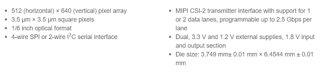
Analog Devices has released an industrial-grade megapixel ToF module ADTF3175 and a VGA resolution sensor the ADSD3030 that seeks to bring the highest accuracy ToF technology in the most compact VGA footprint.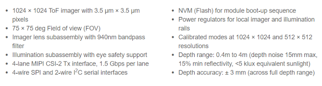
Labforge releases new 20.5T ops/s AI machine vision camera
Image Sensors World Go to the original article...
Labforge has designed and developed a smart camera called Bottlenose which supports 20.5 trillion operations/second processing power and on-board AI, depth, feature points & matching, and a powerful ISP. The target audience is robotics and automation. They have built the camera around a Toshiba Visconti-5 processor. The current models are available as both stereo and monocular versions with IMX577 Sony image sensors. For future models there will be a range of resolutions and shutter options available.


| |||
