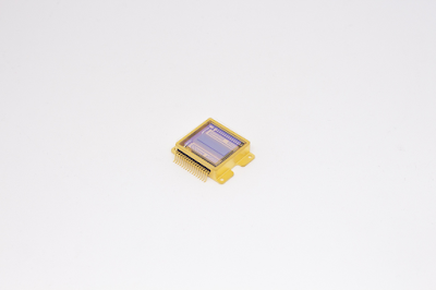
Lynred IR’s new industrial site

Image Sensors World        Go to the original article...

News from: https://ala.associates/funding/lynred-breaks-ground-on-new-e85m-industrial-site-for-infrared-technologies/

Also from Yole: https://www.yolegroup.com/industry-news/lynred-breaks-ground-on-new-e85m-industrial-site-for-infrared-technologies/

Lynred breaks ground on new €85M industrial site for infrared technologies

 Named Campus, Lynred’s new state-of-the-art industrial facility will meet growing market demand for advanced infrared technologies, notably for automotive sector, whilst bolstering French industrial sovereignty in field
 
Company’s production capacity set to undergo 50% increase by 2025; 100% by 2030
 
Grenoble, France, May 10, 2023 – Lynred, a leading global provider of high-quality infrared detectors for the aerospace, defense and commercial markets, today announces breaking ground on its new €85 million ($93.7M) industrial site to produce state-of-the-art infrared technologies. This is the biggest construction investment that the company has undertaken since it began manufacturing in 1986.
 
The project is financed by loans from the CIC bank and Bpifrance.
 
Lynred will double its current cleanroom footprint, totaling 8,200 m2 (88,264 ft2), primarily to meet two strategic objectives:
 Obtain an optimal cleanroom cleanliness classification for its new high-performance products (hybrid detectors)
 Increase the production capacity for its more compact industrial products (bolometers) used in multiple fields, including the automotive industry
This substantial investment will consolidate Lynred’s positioning as European market leader in infrared detection. It enables the company to play a key role within the European defense industrial and technological base, innately woven into strengthening French and European forces, for whom infrared detection is hugely important. With this, Lynred takes a step up in responding to the French government’s call to reorient European industry towards a ‘rearmament economy’ (FR).
 
To mark the ground breaking on May 10, Jean-François Delepau, chairman of Lynred, planted a holm oak tree.
 
“I am delighted to see our state-of-the-art industrial site come to life, consolidating our position as the second largest infrared detector manufacturer in the world. This will enable us to respond to growing market demand for next-generation infrared technologies, including in the automotive sector. It will allow us to contribute to bolstering France’s industrial sovereignty and, more generally, to improve our overall industrial performance. Above all, I wish to thank the Lynred teams involved in this major undertaking, as well as all our partners who have supported us, in particular our shareholders, Thales and Safran. Lynred is embarking on a new strategic pathway, both in terms of technology and dynamic growth,” said Mr Delepau.
 
The buildings are due for completion in the first trimester of 2025 and the site will be fully operational by the following October. This state-of-the-art industrial facility will comprise 8,200 m2 (88,264 ft2) of interconnected cleanrooms (twice the current surface area), 3,400 m2 (36,600ft2) of laboratories, a 2,300 m2 (24,756 ft2) logistics area, and a tertiary and technical area measuring 10,800 m2 (11,625 ft2).
 
Lynred is looking to increase its production capacity by 50% by 2025, in particular for its bolometer products, with a view to doubling capacity by 2030.
 
With these new cleanrooms the company will house all of its French production lines in a single location. This will enable synergies amongst core competencies and optimize production flows.
 
The new buildings will be located on the current Lynred site in Veurey-Voroize, situated within the Grenoble area. They have been designed to ensure optimized energy management and environmental performance: even with 13,600 m2 (146,400 ft2) under construction, the volume of permeable surface will increase. The company will decrease its carbon footprint by 33% and will install 1,800 m2 (19,375 ft2) of solar panels. Moreover, the site will accommodate an additional 320 trees and more than 100 charging stations for electric vehicles (cars and bicycles) will be put in place, with more cycle parking added.
 
About Lynred
Lynred and its subsidiaries, Lynred USA and Lynred Asia-Pacific, are global leaders in designing and manufacturing high quality infrared technologies for aerospace, defense and commercial markets. It has a vast portfolio of infrared detectors that covers the entire electromagnetic spectrum from near to very far infrared. The Group’s products are at the center of multiple military programs and applications. Its IR detectors are the key component of many top brands in commercial thermal imaging equipment sold across Europe, Asia and North America. Lynred is the leading European manufacturer for IR detectors deployed in space.
www.lynred.com


Go to the original article...

ICCP 2023 Call for Demos and Posters

Image Sensors World        Go to the original article...

The call for poster and demo submissions for the IEEE International Conference on Computational Photography (ICCP 2023) is now open. The call is on the website and is available here.

Whereas ICCP papers must describe original research, the posters, and demos give an opportunity to showcase previously published or yet-to-be-published work to a broader community.

The poster track is non-exclusive, and papers submitted to the paper or abstract tracks of ICCP are welcome to present a poster as well.

ICCP is at the rich intersection of optics, graphics, imaging, vision and design. The posters and demos provide an excellent and exciting opportunity for interaction and cross-talk between research communities.

The deadline for posters/demos is June 15, 2023.

Please submit your posters/demos here: https://forms.gle/VdMMEheX1X3ucQG47.

Please refer to the ICCP 2023 website for more information: https://iccp2023.iccp-conference.org/call-for-posters-demos/

Go to the original article...

Review article on figures of merit of 2D photodetectors

Image Sensors World        Go to the original article...

A review article in Nature Communications by Wang et al. (Shanghai Institute of Technical Physics) discusses techniques for characterizing 2D photodetectors.

Full paper: https://www.nature.com/articles/s41467-023-37635-1

Abstract: Photodetectors based on two-dimensional (2D) materials have been the focus of intensive research and development over the past decade. However, a gap has long persisted between fundamental research and mature applications. One of the main reasons behind this gap has been the lack of a practical and unified approach for the characterization of their figures of merit, which should be compatible with the traditional performance evaluation system of photodetectors. This is essential to determine the degree of compatibility of laboratory prototypes with industrial technologies. Here we propose general guidelines for the characterization of the figures of merit of 2D photodetectors and analyze common situations when the specific detectivity, responsivity, dark current, and speed can be misestimated. Our guidelines should help improve the standardization and industrial compatibility of 2D photodetectors. 
Device effective area

a Photoconductive photodetector. b Planar junction photodetector. c, d Vertical junction photodetectors with zero and reverse bias, respectively. e Focal plane photodetector. The dashed blue lines in a–e are suggested accurate effective areas. The dashed orange lines in b, d, and e are potential inaccurate effective areas for respective types. f Field intensity of the Gaussian beam with the beam waist w0 = 2.66 μm, here BP represents black phosphorus. g Wave optics simulation result of the electric field distribution at the upper surface of the device with plane wave injected. h Calculated absorption with the Gaussian beam with the beam waist w0 = 2.66 μm multiplying the wave optics simulation profile shown in (g).


Responsivity

a Monochromatic laser source measurement system, where the laser spot intensity follows the Gaussian distribution. b Relative intensity of the edge of the spot under the researcher’s estimation. The inset shows three spots with the same beam waist and color limit, the only difference of which is the beam intensity. with different intensities and the same beam waist. The estimated radius of spot size shows vast differences. c Laser spot size and power calibration measurement system. d Photon composition of blackbody radiation source, and the radiation distribution in accordance with Planck’s law. e Typical response spectrum of photon detector and thermal detector. The inset shows a diagram of the blackbody measurement system. f Schematic diagram of FTIR measurement system.


Dark current

a Typical dark current mechanism, the dashed lines, filled and empty circles and arrows represent quasi-fermi level, electrons, holes, and carrier transport direction. b Characterization and analysis of dark current for UV-VIS photodetectors. The solid red line is the Id–V characteristic curve measured with a typical VIS photodetector. The green, dark blue, orange, and light blue dashed lines represent the fitted current components of generation-recombination, band-to-band tunneling, diffusion, and trap-assisted tunneling with analytic model. c Dominant dark current for typical photovoltaic photodetectors at different temperatures. d Characterization and analysis of dynamic resistance for infrared photodetectors. The solid red line is the Rd–V characteristic curve measured with a typical infrared photodetector. The orange, green, light blue, and dark blue dashed lines represent the fitted current components of diffusion, generation-recombination, trap-assisted tunneling, and band-to-band tunneling with analytic model. e Dynamic resistance of typical photovoltaic photodetectors at different temperatures.


Other noise sources


a Noise and responsivity characteristics for photodetectors with different response bandwidths for single detection (the blue line represents the typical responsivity curve of photodetectors of high response bandwidth, the green line represents the typical responsivity curve of photodetectors of low response bandwidth, and the red line represents the typical noise characteristics. The vertical dashed lines represent the −3 dB bandwidth for photodetectors with high and low response bandwidth). b Overestimation of specific detectivity based on noise characteristics for single detection. The solid and dashed lines present the calculated specific detectivity with D∗=RAdΔfin from the measured noise and estimated noise of thermal noise and shot noise (ignoring the 1/f noise and g-r noise). c Noise and responsivity characteristics for photodetectors of imaging detection. d Overestimation of specific detectivity based on noise characteristics for imaging detection. The solid and dashed lines present the calculated specific detectivity with D∗=RAdfB∫0fBindf from the measured noise and estimated noise of thermal noise and shot noise (ignoring the 1/f noise and g-r noise).


Time parameters


a Calculated fall time does not reach a stable value which is inaccurate, where τf′ is inaccurate calculated fall time, τf is accurate calculated fall time. (The bule line represents the square signal curve, the yellow line represents the typical response curve of 2D photodetectors.) b Response time measurement of photodetector may not reach a stable value under pulse signal, which will lead to an inaccurate result. The inset shows pulse signal. The τr is inaccurate calculated rise time. c Variation of photocurrent and responsivity of photoconductive photodetectors with the incident optical power density14. d Rise and fall response time of photodetector should be calculated from a complete periodic signal. e Typical −3 dB bandwidth response curve of photodetector, where R0 represents stable responsivity value, fc represents the −3 dB cutoff frequency. f Gain-bandwidth product of various photodetectors, where photo-FET is photo-field-effect transistor, PVFET is photovoltage field-effect transistor14.

Go to the original article...

Sony announces 2022 earnings and 2023 forecast

Image Sensors World        Go to the original article...


Link: https://www.sony.com/en/SonyInfo/IR/library/presen/er/

Go to the original article...

Videos du Jour [onsemi, Sony, Melexis]

Image Sensors World        Go to the original article...


CMOS Image Sensor Layers at a Glance

The onsemi CMOS Image Sensor Wafer consists of the following layers:
• Microlens Array—Small lenses that collect and focus light onto light-sensitive areas of the sensor.
• Color Filter Array (CFA)—Mosaic of tiny color filters placed over the pixel sensors of an image sensor to capture color information.
• Photodiode—Semiconductor that converts light into an electrical current.
• Pixel Transistors—Transistors provide gain or bugger [sic, typo "buffer"?] of electrical charge from the photodiode.
• Bond Layer—Connects the Active Pixel Array to the ASIC layer
• ASIC—Logic layer for features such as error correction, memory for multi-exposures, cores for cybersecurity, hardware blocks for functional safety, and high-speed I/O.


tinyML Summit 2023: Deploying Visual AI Solutions in the Retail Industry

Mark HANSON , VP of Technology and Business Innovation, Sony Semiconductor Solutions of America
An image sensor with AI-processing capability is a novel architecture that is pushing vision AI closer to the edge to enable applications at scale. Today many AI applications stall in the PoC stage and never reach commercial deployment to solve real-world problems because existing systems lack simplicity, flexibility, affordability, and commercial-grade reliability. We’ll investigate why the retail industry struggles to keep track of stock on its retail shelves while relying on retail employees to manually monitor stock and how our (AITRIOS) vision AI application for on-shelf-availability can eliminate complexity and inefficiency at scale.


Melexis: Automotive in-cabin face recognition and anti-spoofing AI using 3D time-of-flight camera

In this demo, we demonstrate in-cabin face recognition and anti-spoofing AI using a 3D time-of-flight camera. Please contact us for more information.

Go to the original article...

Paper on 8-tap ToF Sensor

Image Sensors World        Go to the original article...

Miyazawa et al. from Shizuoka University in Japan recently published an article titled "A Time-of-Flight Image Sensor Using 8-Tap P-N Junction Demodulator Pixels" in the MDPI Sensors journal.

[Open access: https://www.mdpi.com/1424-8220/23/8/3987]

Abstract:
This paper presents a time-of-flight image sensor based on 8-Tap P-N junction demodulator (PND) pixels, which is designed for hybrid-type short-pulse (SP)-based ToF measurements under strong ambient light. The 8-tap demodulator implemented with multiple p-n junctions used for modulating the electric potential to transfer photoelectrons to eight charge-sensing nodes and charge drains has an advantage of high-speed demodulation in large photosensitive areas. The ToF image sensor implemented using 0.11 µm CIS technology, consisting of an 120 (H) × 60 (V) image array of the 8-tap PND pixels, successfully works with eight consecutive time-gating windows with the gating width of 10 ns and demonstrates for the first time that long-range (>10 m) ToF measurements under high ambient light are realized using single-frame signals only, which is essential for motion-artifact-free ToF measurements. This paper also presents an improved depth-adaptive time-gating-number assignment (DATA) technique for extending the depth range while having ambient-light canceling capability and a nonlinearity error correction technique. By applying these techniques to the implemented image sensor chip, hybrid-type single-frame ToF measurements with depth precision of maximally 16.4 cm (1.4% of the maximum range) and the maximum non-linearity error of 0.6% for the full-scale depth range of 1.0–11.5 m and operations under direct-sunlight-level ambient light (80 klux) have been realized. The depth linearity achieved in this work is 2.5 times better than that of the state-of-the-art 4-tap hybrid-type ToF image sensor.


Figure 1. Structure and principle of the two-tap p-n junction demodulator (PND): (a) Top view; (b) Cross-sectional view (X1–X1’); (c) Cross-sectional view (X2–X2’); (d) Potential diagram at the channel (X1–X1’); (e) Potential diagram at Si surface (X2–X2’).


Figure 2. 8-tap demodulation pixel and the operations: (a) Top view of the 8-tap PND; (b) equivalent pixel readout circuits.


Figure 3. 3D device simulation results of the 8-tap PND: (a) X-Y 2D potential plot and carrier traces to transfer to G6; (b) X-Y 2D potential plot and carrier traces to transfer to GD; (c) demodulator top view; (d) 1D potential plot (A–A’) for carrier transfer to floating diffusions, FD6 and FD2; (e) 1D potential plot (B–B’) for carrier transferring to a drain through GD only (red line) and that for carrier transferring to a drain through GD and GDO (black line).


Figure 4. Gate timing and its correspondence to the depth range to be measured: (a) Gate timing when all the gates are activated in every cycle and its correspondence to the distance profile of the back-reflected light intensity; (b) Gate timing when G4–G8 are activated for signal light sampling and G1–G3 are activated for ambient light sampling.


Figure 5. Example of the modified DATA timing diagram for cancelling ambient light.


Figure 6. Chip micrograph.


Figure 7. Response of the 8-tap outputs to the light pulse delay. (a) Response to Short Pulse (940 nm, T0 = 10 ns). (b) Response to Short Pulse (T0 = 10 ns, Normalized). (c) Response to Very Short Pulse (FWHM = 69 ps, 851 nm, Normalized). (d) Time Derivative of (c) by The Delay Time (Normalized). (e) FWHM of The Pixel Response to Very Short Pulse (FWHM = 69 ps) Measured with (d).


Figure 11. Depth image (1.0 m to 11.5 m) while moving a reflector board.


Go to the original article...

Paper on 8-tap ToF Sensor

Image Sensors World        Go to the original article...

Miyazawa et al. from Shizuoka University in Japan recently published an article titled "A Time-of-Flight Image Sensor Using 8-Tap P-N Junction Demodulator Pixels" in the MDPI Sensors journal.

[Open access: https://www.mdpi.com/1424-8220/23/8/3987]

Abstract:
This paper presents a time-of-flight image sensor based on 8-Tap P-N junction demodulator (PND) pixels, which is designed for hybrid-type short-pulse (SP)-based ToF measurements under strong ambient light. The 8-tap demodulator implemented with multiple p-n junctions used for modulating the electric potential to transfer photoelectrons to eight charge-sensing nodes and charge drains has an advantage of high-speed demodulation in large photosensitive areas. The ToF image sensor implemented using 0.11 µm CIS technology, consisting of an 120 (H) × 60 (V) image array of the 8-tap PND pixels, successfully works with eight consecutive time-gating windows with the gating width of 10 ns and demonstrates for the first time that long-range (>10 m) ToF measurements under high ambient light are realized using single-frame signals only, which is essential for motion-artifact-free ToF measurements. This paper also presents an improved depth-adaptive time-gating-number assignment (DATA) technique for extending the depth range while having ambient-light canceling capability and a nonlinearity error correction technique. By applying these techniques to the implemented image sensor chip, hybrid-type single-frame ToF measurements with depth precision of maximally 16.4 cm (1.4% of the maximum range) and the maximum non-linearity error of 0.6% for the full-scale depth range of 1.0–11.5 m and operations under direct-sunlight-level ambient light (80 klux) have been realized. The depth linearity achieved in this work is 2.5 times better than that of the state-of-the-art 4-tap hybrid-type ToF image sensor.


Figure 1. Structure and principle of the two-tap p-n junction demodulator (PND): (a) Top view; (b) Cross-sectional view (X1–X1’); (c) Cross-sectional view (X2–X2’); (d) Potential diagram at the channel (X1–X1’); (e) Potential diagram at Si surface (X2–X2’).


Figure 2. 8-tap demodulation pixel and the operations: (a) Top view of the 8-tap PND; (b) equivalent pixel readout circuits.


Figure 3. 3D device simulation results of the 8-tap PND: (a) X-Y 2D potential plot and carrier traces to transfer to G6; (b) X-Y 2D potential plot and carrier traces to transfer to GD; (c) demodulator top view; (d) 1D potential plot (A–A’) for carrier transfer to floating diffusions, FD6 and FD2; (e) 1D potential plot (B–B’) for carrier transferring to a drain through GD only (red line) and that for carrier transferring to a drain through GD and GDO (black line).


Figure 4. Gate timing and its correspondence to the depth range to be measured: (a) Gate timing when all the gates are activated in every cycle and its correspondence to the distance profile of the back-reflected light intensity; (b) Gate timing when G4–G8 are activated for signal light sampling and G1–G3 are activated for ambient light sampling.


Figure 5. Example of the modified DATA timing diagram for cancelling ambient light.


Figure 6. Chip micrograph.


Figure 7. Response of the 8-tap outputs to the light pulse delay. (a) Response to Short Pulse (940 nm, T0 = 10 ns). (b) Response to Short Pulse (T0 = 10 ns, Normalized). (c) Response to Very Short Pulse (FWHM = 69 ps, 851 nm, Normalized). (d) Time Derivative of (c) by The Delay Time (Normalized). (e) FWHM of The Pixel Response to Very Short Pulse (FWHM = 69 ps) Measured with (d).


Figure 11. Depth image (1.0 m to 11.5 m) while moving a reflector board.


Go to the original article...

Another article on Panasonic’s organic image sensor

Image Sensors World        Go to the original article...

PetaPixel: https://petapixel.com/2023/04/11/panasonics-decade-old-organic-cmos-sensor-is-still-years-away/

Panasonic’s Decade-Old Organic CMOS Sensor is Still Years Away

As a quick reminder, Panasonic's patented technology relies on an organic thin-film photo-conversion material in lieu of the conventional technique where a silicon photodiode converts light into electrical charge.

Some excerpts from the article are below.


... it has been nearly 10 years since the company first announced it was working on this new sensor and in that time, a lot has changed. The previously exciting low light capabilities have since been realized by other sensors...


[In an updated announcement last year Panasonic suggested ...] 8K resolution while retaining those dynamic range promises and would do so at high framerates. More recently, Panasonic explained that the sensor would also feature what is known as “reduced crosstalk,” which basically means that the red, green, and blue pixels of the sensor collect only their intended color and that light, regardless of type and color cast, and won’t spill across each pixel. This results in better color reproduction.
...

Basically, it’s very difficult to get excited about Panasonic’s organic CMOS, and that would be the case even if it was coming to market this year.
...

There are those who have been saying Sigma’s Foveon sensor is stuck in “development hell,” but Panasonic easily has it beat with its organic CMOS. 

Go to the original article...

NEC develops carbon nanotubes-based IR sensor

Image Sensors World        Go to the original article...

From StatNano: https://statnano.com/news/72257/NEC-Develops-the-World's-First-Highly-Sensitive-Uncooled-Infrared-Image-Sensor-Utilizing-Carbon-Nanotubes


NEC Develops the World's First Highly Sensitive Uncooled Infrared Image Sensor Utilizing Carbon Nanotubes

NEC Corporation has succeeded in developing the world's first high-sensitivity uncooled infrared image sensor that uses high-purity semiconducting carbon nanotubes (CNTs) in the infrared detection area. This was accomplished using NEC’s proprietary extraction technology. NEC will work toward the practical application of this image sensor in 2025.


Infrared image sensors convert infrared rays into electrical signals to acquire necessary information, and can detect infrared rays emitted from people and objects even in the dark. Therefore, infrared image sensors are utilized in various fields to provide a safe and secure social infrastructure, such as night vision to support automobiles driving in the darkness, aircraft navigation support systems and security cameras.

There are two types of infrared image sensors, the "cooled type," which operates at extremely low temperatures, and the "uncooled type," which operates near room temperature. The cooled type is highly sensitive and responsive, but requires a cooler, which is large, expensive, consumes a great deal of electricity, and requires regular maintenance. On the other hand, the uncooled type does not require a cooler, enabling it to be compact, inexpensive, and to consume low power, but it has the issues of inferior sensitivity and resolution compared to the cooled type.

(Left) Electron micrograph and image of single-walled CNTs, (Right) Atomic microscope image of a high-purity semiconducting CNT film.


(Left) Device structure, (Right) Photograph of CNT infrared array device.

In 1991, NEC discovered CNTs for the first time in the world and is now a leader in research and development related to nanotechnology. In 2018, NEC developed a proprietary technology to extract only semiconducting-type CNTs at high purity from single-walled CNTs that have a mixture of metallic and semiconducting types. NEC then discovered that thin films of semiconducting-type CNTs extracted with this technology have a large temperature coefficient of resistance (TCR) near room temperature.
The newly developed infrared image sensor is the result of these achievements and know-how. NEC applied semiconductor-type CNTs based on its proprietary technology that features a high TCR, which is an important index for high sensitivity. As a result, the new sensor achieves more than three times higher sensitivity than mainstream uncooled infrared image sensors using vanadium oxide or amorphous silicon.

The new device structure was achieved by combining the thermal separation structure used in uncooled infrared image sensors, the Micro Electro Mechanical Systems (MEMS) device technology used to realize this structure, and the CNT printing and manufacturing technology cultivated over many years for printed transistors, etc. As a result, NEC has succeeded in operating a high-definition uncooled infrared image sensor of 640 x 480 pixels by arraying the components of the structure.

Part of this work was done in collaboration with Japan’s National Institute of Advanced Industrial Science and Technology (AIST). In addition, a part of this achievement was supported by JPJ004596, a security technology research promotion program conducted by Japan’s Acquisition, Technology & Logistics Agency (ATLA).

Going forward, NEC will continue its research and development to further advance infrared image sensor technologies and to realize products and services that can contribute to various fields and areas of society.

Go to the original article...

Sony AITRIOS wins award at tinyML 2023

Image Sensors World        Go to the original article...

Link: https://www.aitrios.sony-semicon.com/en/news/aitrios-to-win-tinyml-awards-2023/ 

At the tinyML Summit 2023, held from March 27 to 29, 2023, Sony Semiconductor Solutions' edge AI sensing platform service, AITRIOS™, won the tinyML Awards 2023 "Best Innovative Software Enablement and Tools".

The tinyML Summit is a global conference on tiny machine learning (TinyML), held since 2019, where business leaders, engineers, and researchers gather to share information on the latest TinyML technologies and applications. This year the conference was held in San Francisco, United States. This award is presented to an individual, team, or organization that has created innovative software tools or development support tools related to TinyML and has contributed to the evolution of this technology.


 Deploying Visual AI Solutions in the Retail Industry
Mark HANSON , VP of Technology and Business Innovation, Sony Semiconductor Solutions of America
An image sensor with AI-processing capability is a novel architecture that is pushing vision AI closer to the edge to enable applications at scale. Today many AI applications stall in the PoC stage and never reach commercial deployment to solve real-world problems because existing systems lack simplicity, flexibility, affordability, and commercial-grade reliability. We’ll investigate why the retail industry struggles to keep track of stock on its retail shelves while relying on retail employees to manually monitor stock and how our (AITRIOS) vision AI application for on-shelf-availability can eliminate complexity and inefficiency at scale.

About AITRIOS:

The name “AITRIOS” consists of the platform keyword “AI” and “Trio S,” meaning, “three S’s.” Through AITRIOS, SSS aims to deliver the three S’s of “Solution,” “Social Value,” and “Sustainability” to the world.

Through this platform, SSS seeks to facilitate development of optimal systems, in which the edge and the cloud function in synergy, to support its partners in popularizing and expanding environmentally conscious sensing solutions using edge AI, and to deliver new value and help solve challenges faced by various industries.


AITRIOS integrates an AI model and application development environment, a marketplace, cloud-based services , and other items required for solution development into a powerful and flexible platform.

SSS, a leading company in image sensors, offers sensor configurations optimized for edge AI, enabling partners to build high-performance and reliable solutions.

AITRIOS is a one-stop B2B* (business to business) platform providing tools and environments that facilitate software and application development and system implementation.

*This service is not currently available to individual customers.

Go to the original article...

Canon’s 3.2 MP SPAD Camera: Specifications

Image Sensors World        Go to the original article...

Canon's 3.2 MP SPAD camera has received some press coverage:

PetaPixel: https://petapixel.com/2023/04/03/canons-new-sensor-enables-long-range-night-vision-capabilities/

YMCinema: https://ymcinema.com/2023/04/03/canon-develops-interchangeable-lens-camera-that-sees-in-the-dark/ 

Unfortunately I have not been able to find a spec sheet. The next best thing for now is to see the 2021 IEDM proceedings paper titled "3.2 Megapixel 3D-Stacked Charge Focusing SPAD for Low-Light Imaging and Depth Sensing" (Morimoto et al., Canon Inc., Japan).  Thanks to Prof. Eric Fossum for pointing this out in a comment on an earlier post!

Abstract:
We present a new generation of scalable photon counting image sensors, featuring zero read noise and 100ps temporal resolution. Newly proposed charge focusing single-photon avalanche diode (SPAD) is employed to resolve critical trade-offs in conventional SPAD pixels. A prototype 3.2 megapixel 3D-stacked backside-illuminated (BSI) image sensor with 1-inch format demonstrates the best-in-class photon detection efficiency (PDE), dark count rate (DCR) and timing jitter performance with the largest array size ever reported in avalanche photodiode (APD)-based image sensors. The proposed technology paves the way to compact and high-definition photon counting image sensors for low-light imaging and 3D time-of-flight sensing.


Go to the original article...

"ai-CMOS" 9-channel color camera

Image Sensors World        Go to the original article...

From Transformative Optics Corporation: https://www.ai-cmos.com/

ai-CMOS sensors solve many of today’s challenges with antiquated CMOS technology, offering unprecedented accuracy, an expanded spectrum, plus 9-channel AI-optimized color. Extending beyond the visible spectrum into near-ultraviolet (NUV) and near-infrared (NIR) greatly expands capabilities for mobile photography, autonomous transport, and machine vision.

With higher sensitivity than Bayer sensors, near-complete color gamut, and expansion beyond visible light to near-infrared and ultraviolet frequencies, ai-CMOS brings a unique multispectral ability to standard cameras.


Mobile Photography.
Close the gap between performance and portability, while unlocking new potential for AI-powered apps.
More Contrast: Improved Black and White Modulation Transfer Function (MTF)
Broader Spectrum: Extension to Near Infrared (NIR) and Near Ultraviolet channel
Near-Complete Color Gamut: Improving color accuracy, automated white balance
Enhanced Sensitivity: Twice the Light. Lower light levels, less motion blur, plus twice the signal levels for a myriad of Integrated Signal Processing functions.

Machine Vision.
ai-CMOS offers AI applications richer and more complete data sets for training, object detection, and object classification.
Richer Data: 3x the information over Bayer
AI Optimizations: increased raw data content for feature vectors and 2x the signal strength for Integrated Signal Processing aiding apps like Super-Resolution
More Contrast: Improved Black and White Modulation Transfer Function (MTF)
Broader Spectrum: Extension to Near Infrared (NIR) and Near Ultraviolet channels

Automotive.
ai-CMOS captures more detailed data in low-light conditions, at night, and in poorer weather conditions, like fog and rain.
Spectral Sensitivity: ai-CMOS captures twice the light of current ADAS CMOS technology on the market.
Object Detection: 25% color gamut increase and 3x Feature Vectors from traditional sensors, greatly enhancing object detection and classification.
Autonomous Driving: Better enable autonomous vehicles to navigate more complex environments, and interact with other vehicles and pedestrians.


Sensor Specs.

Resolution: 3000 x 3864
Pixel Size: 8um
Sensor Format: 35mm (dia. 39.3mm)
Spectral Response: 350nm to 850nm
Quantum Efficiency: >90%
Illumination-type: BSI
Frame Rate: 30fps in HDR
Full Well: >65,000 e-
Gain Mode: HDR and Dual Gain
 

Available in limited quantities in 2023.

Go to the original article...

SWIR imaging market ‘worth $2.9BN by 2028’

Image Sensors World        Go to the original article...

From optics.org news: https://optics.org/news/14/4/15

12 Apr 2023
Yole Intelligence says that the war in Ukraine and tensions over Taiwan will push defense applications beyond prior expectations.

Analysts at France-based Yole Intelligence say the current niche market for short-wave infrared (SWIR) imaging technology will grow rapidly over the next five years, and will be worth $2.9 billion by 2028.

In a new report on the segment, which is currently dominated by applications in defense, research, and industry, Yole’s Alex Clouet suggests that SWIR technology could begin replacing near-infrared (NIR) imagers in high-end smart phones, where the technology is used for secure identification.
Together with higher growth than previously expected in the military arena, plus innovation in key component materials expected to reduce costs, the upshot is expected to be a compound annual growth rate in excess of 40 per cent over the next few years.


Although definitions of SWIR and NIR spectral ranges differ, the term SWIR is often used to refer to wavelengths between 1400 nm and 3000 nm, whereas NIR relates to the 780-1400 nm band.
According to the report, the SWIR imaging market was worth just over $300 million last year, with defense, aerospace, and research applications accounting for more than two-thirds of that total.
“The defense segment will experience higher growth than previously expected, reaching $405 million in 2028 from $228 million in 2022, pulled by geopolitical tensions such as the Ukraine war and tensions around Taiwan and an increasing number of countries becoming interested in SWIR technologies,” Yole says.

The current focus means that defense-oriented players such as Israel’s SCD, Sensors Unlimited, and Teledyne FLIR dominate the scene. But as the technology begins to find use in a larger number of industrial and consumer applications, that is likely to change.

“Many smaller players have significant growth potential, like Sony, or companies making quantum-dot-based cameras, such as SWIR Vision Systems and Emberion, which have a price advantage on high-resolution and extended spectral range products,” Yole stated.

“Newcomers bring new disruptive technologies, like STMicroelectronics, TriEye, or Artilux, to address consumer or automotive markets.”

Emberion, which is a spin-out from Nokia with facilities in Cambridge, UK, uses both colloidal quantum dots and graphene in its devices - claiming improvements in signal-to-noise, breadth of spectral response, and operating temperature.

“Traditional CMOS image sensor suppliers can be game-changers due to their high-volume production capacity and unique design and integration know-how,” observes Yole.
“However, among them, only Sony and STMicroelectronics have already developed SWIR imaging technology - even though others may show signs of interest, such as Samsung and OmniVision.
“The SWIR ecosystem waits for greater interest from these players to accelerate technological and market disruption.”


Material innovation
Nevertheless, the technology is expected to make an impact in consumer goods, with Yole’s figures suggesting the emergence of a significant consumer market over the next five years.
“In 2026, SWIR can start replacing NIR imagers in flagship smart phones for under-display integration of facial recognition modules,” reckons Clouet, adding that the resulting market for complete 3D-sensing modules will just surpass $2 billion by 2028.
Beyond that - and depending on the level of innovation and cost reductions in key components - the technology might end up being integrated into lower-end smart phones and augmented and virtual reality (AR/VR) headsets to improve the performance of tracking cameras, 3D sensing, and outdoor multispectral imaging.

Clouet also sees applications emerging in the automotive sector, where SWIR could provide enhanced vision in low light and adverse weather conditions, as well as 3D sensing capability - although this market would still be in its infancy by 2028.

Among the technological innovations that may lead to more efficient and lower-cost imaging systems, Yole highlights the potential of quantum dots, organic photodiodes, and the germanium-on-silicon material system as some potentially key developments in sensors.
At the optical component level, polymer and metasurface lenses, diffractive optics and optical diffusers, and spectral filters could also contribute to lower costs.

Yole's report, SWIR Imaging 2023, is available now via the company’s web site.


Go to the original article...

SWIR linear array sensor from NIT

Image Sensors World        Go to the original article...

Press release from NIT:


The NSC1801 line scan sensor was designed initially for imaging linearly moving objects with high frame rate, high sensitivity and low noise. Its pixel size has the world smallest size of 7.5µm that contributes the lower the manufacturing costs without increasing the cost of lenses.

Now NIT is pleased to release an updated version of NSC1801, where all key parameters have been reworked and overall performances improved. NSC1801 is currently installed in NIT Lisa SWIR cameras.

NSC1801 fully benefits from NIT new manufacturing factory installed in our brand new clean room, that includes our high yield hybridization process. Our new facility allows to cover the full design and manufacturing cycle of these sensors in volume with a level of quality never achieved before. 

Moreover NSC1801 was designed with the objective of addressing new markets that could not invest into expensive and difficult to use SWIR cameras. The result is that our Lisa SWIR camera based on NSC1801 exhibits the lowest price point on the market even in unit quantity.  

Typical applications for NSC1801 are waste sorting, semiconductor and photovoltaic cell inspection, food and vegetable inspection and pharmaceutical inspection. 


Features

Benefits

Pixel size 7.5x7.5µm

Lowest pixel size in the industry to capture sharp details

Resolution 2048 pixels

Large field of view compatible with most lenses from the market

Three gain modes available

Allows selecting the best dynamic range for the scene. 

QE >85%

Boost sensitivity to the maximum available

Line rate up to 60KHz

For imaging fast moving objects 

Exposure time 10µs to 220ms

Fully configurable for capturing the best signal to noise ratio


Go to the original article...

Canon to start selling 3.2MP SPAD sensor in 2023

Image Sensors World        Go to the original article...

Canon developing world-first ultra-high-sensitivity ILC equipped with SPAD sensor, supporting precise monitoring through clear color image capture of subjects several km away, even in darkness

TOKYO, April 3, 2023—Canon Inc. announced today that the company is developing the MS-500, the world's first1 ultra-high-sensitivity interchangeable-lens camera (ILC) equipped with a 1.0 inch Single Photon Ava