Panasonic introduces high sensitivity hyperspectral imager

Image Sensors World        Go to the original article...

From Imaging and Machine Vision Europe: https://www.imveurope.com/news/panasonic-develops-low-light-hyperspectral-imaging-sensor-worlds-highest-sensitivity 

Panasonic develops low-light hyperspectral imaging sensor with "world's highest" sensitivity

Panasonic has developed what it says is the world's highest sensitivity hyperspectral imaging technology for low-light conditions.

Based on a ‘compressed’ sensor technology previously used in medicine and astronomy, the technology was first demonstrated last month in Nature Photonics.

Conventional hyperspectral imaging technologies use optical elements such as prisms and filters to selectively pass and detect light of a specific wavelength assigned to each pixel of the image sensor. However, these technologies have a physical restriction in that light of the non-assigned wavelengths cannot be detected at each pixel, decreasing the sensitivity inversely proportional to the number of wavelengths being captured.

Therefore, illumination with a brightness comparable to that of the outdoors on a sunny day (10,000 lux or more) is required to use such technologies, which decreases their usability and versatility.

The newly developed hyperspectral imaging technology instead employs ‘compressed’ sensing, which efficiently acquires images by "thinning out" the data and then reconstructing it. Such techniques have previously been deployed in medicine for MRI examinations, and in astronomy for black hole observations.

A distributed Bragg reflector (DBR) structure that transmits multiple wavelengths of light is implemented on the image sensor. This special filter transmits around 45% of incident light, between 450-650nm, and is divided into 20 wavelengths. It offers a sensitivity around 10-times higher than conventional technologies, which demonstrate a light-use efficiency of less than 5%. The filter is designed to appropriately thin out the captured data by transmitting incident light with randomly changing intensity for each pixel and wavelength. The image data is then reconstructed rapidly using a newly optimised algorithm. By leaving a part of the colour-separating functions to the software, Panasonic has been able to overcome the previous trade-off between the number of wavelengths and sensitivity – the fundamental issue of conventional hyperspectral technologies. 

This approach has made it possible to capture hyperspectral images and video with what Panasonic says is the world's highest sensitivity, under indoor levels of illumination (550 lux). This level of sensitivity enables a fast shutter speed of more than 30fps, previously unachievable using conventional hyperspectral technologies due to their low sensitivity and consequently low frame rate. This significantly increases the new technology’s usability due it being easier to focus and align.

Application examples of the new technology, which was initially demonstrated alongside Belgian research institute Imec, include the inspection of tablets and foods, as this can now be done without the risk of the previously-required high levels of illumination raising their temperature.


Go to the original article...

Sony’s high-speed camera interface standard SLVS-EC

Image Sensors World        Go to the original article...

https://www.sony-semicon.com/en/technology/is/slvsec.html?cid=em_nl_20230228 

Scalable Low-Voltage Signaling with Embedded Clock (SLVS-EC), is a high-speed interface standard developed by Sony Semiconductor Solutions Corporation (SSS) for fast, high-resolution image sensors. The interface's simple protocol makes it easy to build camera systems. Featuring an embedded clock signal, it is ideal for applications that require larger capacity, higher speed, or transmission over longer distances. While introducing a wide range of SLVS-EC compliant products, SSS will continue to promote SLVS-EC as a standard of interface for industrial image sensors that face increasing demands for more pixels and higher speed.


Enables implementation for high-speed, high-resolution image sensors without adding pins or enlarging the package. Supports up to 5 Gbps/lane. (As of November 2020.)

Uses the same 8b/10b encoding as in common interfaces. Can be connected to FPGAs or other common industrial camera components. With an embedded clock signal, SLVS-EC requires no skew adjustment between lanes and is a good choice for long-distance transmission. Simple protocol facilitates implementation.

SLVS-EC is standardized by the Japan Industrial Imaging Association (JIIA)

Go to the original article...

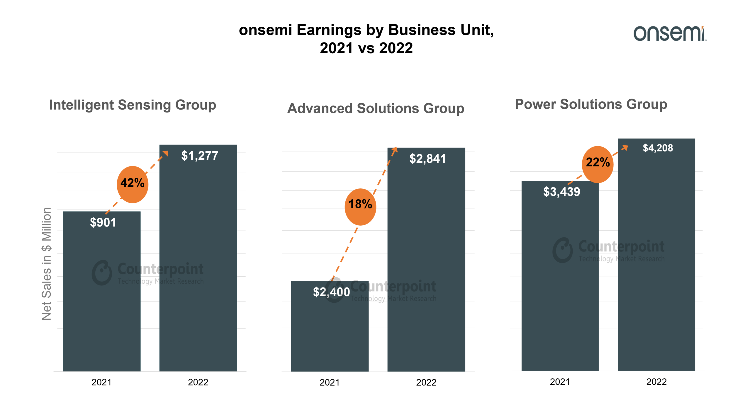
ON Semi sensor sales jumped up by 42% in 2022

Image Sensors World        Go to the original article...

From Counterpoint Research: https://www.counterpointresearch.com/sensing-power-solutions-drive-onsemis-record-revenue-in-2022/

Sensing, Power Solutions Drive onsemi’s Record Revenue in 2022


2022 highlights
  • Delivered a record revenue of $8.3 billion at 24% YoY growth, primarily driven by strength in automotive and industrial businesses.
  • Reduction in price-to-value discrepancies, exiting volatile and competitive businesses and pivoting portfolio to high-margin products helped onsemi deliver strong earnings.
  • Revenue from auto and industrial end-markets increased 38% YoY to $ 4 billion and accounted for 68% of total revenues.
  • Intelligent Sensing Group revenue increased 42% YoY to $1.28 billion driven by the transition to higher-resolution sensors at elevated ASPs.
  • Non-GAAP gross margin was at 49.2%, an increase of 880 basis points YoY. The expansion was driven by manufacturing efficiencies, favorable mix and pricing, and reallocation of capacity to strategic and high-margin products.
  • Revenue from silicon carbide (SiC) shipments in 2022 was more than $200 million.
  • Revenue committed from SiC solutions through LTSAs increased to $4.5 billion.
  • Total LTSAs across the entire portfolio were at $16.6 billion exiting 2022.
  • Revenue from new product sales increased by 34% YoY.
  • Design wins increased 38% YoY.

Go to the original article...

Stanford University talk on Pixel Design

Image Sensors World        Go to the original article...

Dan McGrath (Senior Consultant) recently gave a talk titled "Insider’s View on Pixel Design" at the Stanford Center for Image Systems Engineering (SCIEN), Stanford University. It is survey of challenges based on Dan's 40+ years of experience.

The full 1+ hour talk is available here:

Description:
The success of solid state image sensors has been the cost-effective integrating mega-arrays of transducers into the design flow and manufacturing process that has been the basis of the success of integrated circuits in our industry, This talk will provide from a front-line designer’s perspective key challenges that have been overcome and that still exist to enable this: device physics, integration, manufacturing, meeting customer expectations.

Further Information:
Dan McGrath has worked for over 40 years specializing in the device physics of pixels, both CCD and CIS, and in the integration of image-sensor process enhancements in the manufacturing flow. He received his doctorate in physics from John Hopkins University. He chose his first job because it offered that designing image sensors “means doing physics” and has kept this passion front-and-center in his work. He has worked at Texas Instruments, Polaroid, Atmel, Eastman Kodak, Aptina, BAE Systems and GOODiX Technology and with manufacturing facilities in France, Italy, Taiwan, China and the USA. He has been involved with astronomers on the Galileo mission to Jupiter and to Halley’s Comet, with commercial companies on cell phone imagers and biometrics, with scientific community for microscopy and lab-on-a-chip, with robotics on 3-d mapping sensors and with defense contractors on night vision. His publications include the first megapixel CCD and the basis for dark current spectroscopy (DCS).


Go to the original article...

Ambient light resistant long-range time-of-flight sensor

Image Sensors World        Go to the original article...

Kunihiro Hatakeyama et al. of Toppan Inc. and Brookman Technology Inc. (Japan) published an article titled "A Hybrid ToF Image Sensor for Long-Range 3D Depth Measurement Under High Ambient Light Conditions" in the IEEE Journal of Solid-State Circuits.

Abstract: 

A new indirect time of flight (iToF) sensor realizing long-range measurement of 30 m has been demonstrated by a hybrid ToF (hToF) operation, which uses multiple time windows (TWs) prepared by multi-tap pixels and range-shifted subframes. The VGA-resolution hToF image sensor with 4-tap and 1-drain pixels, fabricated by the BSI process, can measure a depth of up to 30 m for indoor operation and 20 m for outdoor operation under high ambient light of 100 klux. The new hToF operation with overlapped TWs between subframes for mitigating an issue on the motion artifact is implemented. The sensor works at 120 frames/s for a single subframe operation. Interference between multiple ToF cameras in IoT systems is suppressed by a technique of emission cycle-time changing.


Full paper: https://doi.org/10.1109/JSSC.2023.3238031

Go to the original article...

PetaPixel article on limits of computational photography

Image Sensors World        Go to the original article...

Full article: https://petapixel.com/2023/02/04/the-limits-of-computational-photography/

Some excerpts below:

On the question of whether dedicated cameras are better than today's smartphone cameras the author argues:
“yes, dedicated cameras have some significant advantages”. Primarily, the relevant metric is what I call “photographic bandwidth” – the information-theoretic limit on the amount of optical data that can be absorbed by the camera under given photographic conditions (ambient light, exposure time, etc.).

Cell phone cameras only get a fraction of the photographic bandwidth that dedicated cameras get, mostly due to size constraints. 
 
There are various factors that enable a dedicated camera to capture more information about the scene:
  • Objective Lens Diameter
  • Optical Path Quality
  • Pixel Size and Sensor Depth
Computational photography algorithms try to correct the following types of errors:
  • “Injective” errors. Errors where photons end up in the “wrong” place on the sensor, but they don’t necessarily clobber each other. E.g. if our lens causes the red light to end up slightly further out from the center than it should, we can correct for that by moving red light closer to the center in the processed photograph. Some fraction of chromatic aberration is like this, and we can remove a bit of chromatic error by re-shaping the sampled red, green, and blue images. Lenses also tend to have geometric distortions which warp the image towards the edges – we can un-warp them in software. Computational photography can actually help a fair bit here.
  • “Informational” errors. Errors where we lose some information, but in a non-geometrically-complicated way. For example, lenses tend to exhibit vignetting effects, where the image is darker towards the edges of the lens. Computational photography can’t recover the information lost here, but it can help with basic touch-ups like brightening the darkened edges of the image.
  • “Non-injective” errors. Errors where photons actually end up clobbering pixels they shouldn’t, such as coma. Computational photography can try to fight errors like this using processes like deconvolution, but it tends to not work very well.
The author then goes on to criticize the practice of imposing too strong a "prior" in computational photography algorithms, so much that the camera might "just be guessing" what the image looks like with very little real information about the scene. 

Go to the original article...

TRUMPF industrializes SWIR VCSELs above 1.3 micron wavelength

Image Sensors World        Go to the original article...

From Yole industry news: https://www.yolegroup.com/industry-news/trumpf-reports-breakthrough-in-industrializing-swir-vcsels-above-1300-nm/

TRUMPF reports breakthrough in industrializing SWIR VCSELs above 1300 nm

TRUMPF Photonic Components, a global leader in VCSEL and photodiode solutions, is industrializing the production of SWIR VCSELs above 1300 nm to support high volume applications such as in smartphones in under-OLED applications. The company demonstrates outstanding results regarding the efficiency of infrared laser components with long wavelengths beyond 1300 nm on an industrial-grade manufacturing level. This takes TRUMPF one step further towards mass production of indium-phosphide-based (InP) VCSELs in the range from 1300 nm to 2000 nm. “At TRUMPF we are working hard to mature this revolutionary production process and to implement standardization, which would further develop this outstanding technology into a cost-attractive solution. We aim to bring the first products to the high-volume market in 2025,” said Berthold Schmidt, CEO at TRUMPF Photonic Components. By developing the new industrial production platform, TRUMPF is expanding its current portfolio of Gallium arsenide- (GaAs-) based VCSELs in the 760 nm to 1300 nm range for NIR applications. The new platform is more flexible in the longer wavelength spectrum than are GaAs, but it still provides the same benefits as compact, robust and economical light sources. “The groundwork for the successful implementation of long-wavelength VCSELs in high volumes has been laid. But we also know that it is still a way to go, and major production equipment investments have to be made before ramping up mass production”, said Schmidt.

VCSELs to conquer new application fields

A broad application field can be revolutionized by the industrialization of long-wavelength VCSELs, as the SWIR VCSELs can be used in applications with higher output power while remaining eye-safe compared to shorter-wavelength VCSELs. The long wavelength solution is not susceptible to disturbing light such as sunlight in a broader wavelength regime. One popular example from the mass markets of smartphone and consumer electronics devices, is under-OLED applications. The InP-based VCSELs can be easily put below these OLED displays, without disturbing other functionalities and with the benefit of higher eye-safety standards. OLED displays are a huge application field for long wavelength sensor solutions. “In future we expect high volume projects not only in the fields of consumer sensing, but automotive LiDAR, data communication applications for longer reach, medical applications such as spectroscopy applications, as well as photonic integrated circuits (PICs), and quantum photonic integrated circuits (QPICs). The related demands enable the SWIR VCSEL technology to make a breakthrough in mass production”, said Schmidt.

Exceptional test results

TRUMPF presents results showing VCSEL laser performance up to 140°C at ~1390 nm wavelength. The technology used for fabrication is scalable for mass production and the emission wavelength can be tuned between 1300 nm to 2000 nm, resulting in a wide range of applications. Recent results show good reproducible behavior and excellent temperature performance. “I’m proud of my team, as it’s their achievement that we can present exceptional results in the performance and robustness of these devices”, said Schmidt. “We are confident that the highly efficient, long wavelength VCSELs can be produced at high yield to support cost-effective solutions”, Schmidt adds.

Go to the original article...

ON Semi announces that it will be manufacturing image sensors in New York

Image Sensors World        Go to the original article...

Press release: https://www.onsemi.com/company/news-media/press-announcements/en/onsemi-commemorates-transfer-of-ownership-of-east-fishkill-new-york-facility-from-globalfoundries-with-ribbon-cutting-ceremony

onsemi Commemorates Transfer of Ownership of East Fishkill, New York Facility from GlobalFoundries with Ribbon Cutting Ceremony

  • Acquisition and investments planned for ramp-up at the East Fishkill (EFK) fab create onsemi’s largest U.S. manufacturing site
  • EFK enables accelerated growth and differentiation for onsemi’s power, analog and sensing technologies
  • onsemi retains more than 1,000 jobs at the site
PHOENIX – Feb. 10, 2023 – onsemi (Nasdaq: ON) a leader in intelligent power and sensing technologies, today announced the successful completion of its acquisition of GlobalFoundries’ (GF’s) 300 mm East Fishkill (EFK), New York site and fabrication facility, effective December 31, 2022. The transaction added more than 1,000 world-class technologists and engineers to the onsemi team. Highlighting the importance of manufacturing semiconductors in the U.S., the company celebrated this milestone event with a ribbon-cutting ceremony led by Senate Majority Leader Chuck Schumer (NY), joined by Senior Advisor to the Secretary of Commerce on CHIPS Implementation J.D. Grom. Also in attendance were several other local governmental dignitaries.

Over the last three years, onsemi has been focusing on securing a long-term future for the EFK facility and its employees, making significant investments in its 300 mm capabilities to accelerate growth in the company’s power, analog and sensing products, and enable an improved manufacturing cost structure. The EFK fab is the largest onsemi manufacturing facility in the U.S., adding advanced CMOS capabilities - including 40 nm and 65 nm technology nodes with specialized processing capabilities required for image sensor production - to the company’s manufacturing profile. The transaction includes an exclusive commitment to supply GF with differentiated semiconductor solutions and investments in research and development as both companies collaborate to build on future growth.

“With today’s ribbon cutting, onsemi will preserve more than 1,000 local jobs, continue to boost the state’s leadership in the semiconductor industry, and supply ‘Made in New York' chips for everything from electric vehicles to energy infrastructure across the country,” said Senator Schumer. “I am elated that onsemi has officially made East Fishkill home to its leading and largest manufacturing fab in the U.S. onsemi has already hired nearly 100 new people and invested committed $1.3 billion to continue the Hudson Valley’s rich history of science and technology for future generations. I have long said that New York had all the right ingredients to rebuild our nation’s semiconductor industry, and personally met with onsemi’s top brass multiple times to emphasize this as I was working on my historic CHIPS legislation. Thanks to my CHIPS and Science Act, we are bringing manufacturing back to our country and strengthening our supply chains with investments like onsemi’s in the Hudson Valley.”

The EFK facility contributes to the community by retaining more than 1,000 jobs. With the recent passage of the Federal CHIPS and Science Act as well as the New York Green CHIPS Program, onsemi will continue to evaluate opportunities for expansion and growth in East Fishkill and its contribution to the surrounding community. Earlier today, the Rochester Institute of Technology (RIT) announced that onsemi has pledged to donate $500,000 over 10 years to support projects and education aimed at increasing the pipeline of engineers in the semiconductor industry.

“onsemi appreciates Senate Majority Leader Schumer’s unwavering commitment to ensure American leadership in semiconductors and chip manufacturing investments in New York,” said Hassane El-Khoury, president and chief executive officer, onsemi. “With the addition of EFK to our manufacturing footprint, onsemi will have the only 12-inch power discrete and image sensor fab in the U.S., enabling us to accelerate our growth in the megatrends of vehicle electrification, ADAS, energy infrastructure and factory automation. We look forward to working with Empire State Development and local government officials to find key community programs and educational partnerships that will allow us to identify, train and employ the next generation of semiconductor talent in New York.”

Go to the original article...

ST introduces new sensors for computer vision, AR/VR

Image Sensors World        Go to the original article...


ST has released a new line of global shutter image sensors with embedded optical flow feature which is fully autonomous with no need for host computing/assistance. This can provide savings in power and bandwidth and free up host resources that would otherwise be needed for optical flow computations. From this optical flow data, it is possible for a host processor to compute the visual odometry (SLAM or camera trajectory), without the need for the full RGB image. The optical flow data can be interlaced with the standard image stream, with any of the monochrome, RGB Bayer or RGB-IR sensor versions. 

Go to the original article...

Canon Announces 148dB (24 f-stop) Dynamic Range Sensor

Image Sensors World        Go to the original article...

Canon develops CMOS sensor for monitoring applications with industry-leading dynamic range, automatic exposure optimization function for each sensor area that improves accuracy for recognizing moving subjects


TOKYO, January 12, 2023—Canon Inc. announced today that the company has developed a 1.0-inch, back-illuminated stacked CMOS sensor for monitoring applications that achieves an effective pixel count of approximately 12.6 million pixels (4,152 x 3,024) and provides an industry-leading1 dynamic range of 148 decibels2 (dB). The new sensor divides the image into 736 areas and automatically determines the best exposure settings for each area. This eliminates the need for synthesizing images, which is often necessary when performing high-dynamic-range photography in environments with significant differences in brightness, thereby reducing the amount of data processed and improving the recognition accuracy of moving subjects.


With the increasingly widespread use of monitoring cameras in recent years, there has been a corresponding growth in demand for image sensors that can capture high-quality images in environments with significant differences in brightness, such as stadium entrances and nighttime roads. Canon has developed a new sensor for such applications, and will continue to pursue development of sensors for use in a variety of fields.

The new sensor realizes a dynamic range of 148 dB—the highest-level performance in the industry among image sensors for monitoring applications. It is capable of image capture at light levels ranging from approximately 0.1 lux to approximately 2,700,000 lux. The sensor's performance holds the potential for use in such applications as recognizing both vehicle license plates and the driver's face at underground parking entrances during daytime, as well as combining facial recognition and background monitoring at stadium entrances.

 1Among market for CMOS sensors used in monitoring applications. As of January 11, 2023. Based on Canon research.

 2Dynamic range at 30 fps is 148 dB. Dynamic range at approx. 60 fps is 142 dB.

In order to produce a natural-looking image when capturing images in environments with both bright and dark areas, conventional high-dynamic-range image capture requires taking multiple separate photos under different exposure conditions and then synthesizing them into a single image. Because exposure times vary in length, this synthesis processing often results in a problem called "motion artifacts," in which images of moving subjects are merged but do not overlap completely, resulting in a final image that is blurry. Canon's new sensor divides the image into 736 distinct areas, each of which can automatically be set to the optimal exposure time based on brightness level. This prevents the occurrence of motion artifacts and makes possible facial recognition with greater accuracy even when scanning moving subjects. What's more, image synthesizing is not required, thereby reducing the amount of data to be processed and enabling high-speed image capture at speeds of approximately 60 frames-per-second3 (fps) and a high pixel count of approximately 12.6 million pixels.

 3Dynamic range at 30 fps is 148 dB. Dynamic range at approx. 60 fps is 142 dB.

Video is comprised of a series of individual still images (single frames). However, if exposure conditions for each frame is not specified within the required time for that frame, it becomes difficult to track and capture images of subjects in environments with subject to significant changes in brightness, or in scenarios where the subject is moving at high speeds. Canon's new image sensor is equipped with multiple CPUs and dedicated processing circuitry, enabling it to quickly and simultaneously specify exposure conditions for all 736 areas within the allotted time per frame. In addition, image capture conditions can be specified according to environment and use case. Thanks to these capabilities, the sensor is expected to serve a wide variety of purposes including fast and highly accurate subject detection on roads or in train stations, as well as stadium entrances and other areas where there are commonly significant changes in brightness levels.

Example use case for new sensor
  • Parking garage entrance, afternoon: With conventional cameras, vehicle's license plate is not legible due to whiteout, while driver's face is not visible due to crushed blacks. However, the new sensor enables recognition of both the license plate and driver's face.
  • The new sensor realizes an industry-leading high dynamic range of 148 dB, enabling image capture in environments with brightness levels ranging from approx. 0.1 lux to approx. 2,700,000 lux. For reference, 0.1 lux is equivalent to the brightness of a full moon at night, while 500,000 lux is equivalent to filaments in lightbulbs and vehicle headlights.


Technology behind the sensor's wide dynamic range

With conventional sensors, in order to produce a natural-looking image when capturing images in environments with both bright and dark areas, high-dynamic-range image capture requires taking multiple separate photos under different exposure conditions and then synthesizing them into a single image. (In the diagram below, four exposure types are utilized per single frame).

With Canon's new sensor, optimal exposure conditions are automatically specified for each of the 736 areas, thus eliminating the need for image synthesis.


Technology behind per-area exposure

Portion in which subject moves is detected based on discrepancies between first image (one frame prior) and second image (two frames prior). ((1) Generate movement map).

In first image (one frame prior) brightness of subject is recognized for each area4 and luminance map is generated (2). After ensuring difference in brightness levels between adjacent areas are not excessive ((3) Reduce adjacent exposure discrepancy), exposure conditions are corrected based on information from movement map, and final exposure conditions are specified (4).

Final exposure conditions (4) are applied to images for corresponding frames.


4 Diagram below is a simplified visualization. Actual sensor is divided into 736 areas.


Go to the original article...

New SWIR Sensor from NIT

Image Sensors World        Go to the original article...


NSC2001 is the NIT Triple H SWIR sensor:
  • High Dynamic Range operating in linear and logarithmic mode response, it exhibits more than 120 dB of dynamic range
  • High Speed, capable of generating up to 1K frames per second in full frame mode, and much more with sub windowing
  • High Sensitivity and low noise figure (< 50e-)


NSC2001 fully benefits from NIT’s new manufacturing factory installed in their brand-new clean room, which includes their high-yield hybridization process. The new facility allows NIT to cover the entire design and manufacturing cycle of these sensors in volume with a level of quality never achieved before.

Moreover, NSC2001 was designed with the objective of addressing new markets that could not invest in expensive and difficult-to-use SWIR cameras. The result is that our WiDy SenS 320 camera based on NSC2001 exhibits the lowest price point on the market even in unit quantity.

Typical applications for NSC2001 are optical metrology and testing, additive manufacturing, welding, & laser communication, etc.

Go to the original article...

Workshop on Infrared Detection for Space Applications June 7-9, 2023 in Toulouse, France

Image Sensors World        Go to the original article...

CNES, ESA, ONERA, CEA-LETI, Labex Focus, Airbus Defence & Space and Thales Alenia Space are pleased to inform you that they are organising the second workshop dedicated to Infrared Detection for Space Applications, that will be held in Toulouse from 7th to 9th, June 2023 in the frame of the Optics and Optoelectronics Technical Expertise Community (COMET).

The aim of this workshop is to focus on Infrared Detectors technologies and components, Focal Plane Arrays and associated subsystems, control and readout ASICs, manufacturing, characterization and qualification results. The workshop will only address IR spectral bands between 1μm and 100 μm. Due to the commonalities with space applications and the increasing interest of space agencies to qualify and to use COTS IR detectors, companies and laboratories involved in defence applications, scientific applications and non-space cutting-edge developments are very welcome to attend this workshop.

The workshop will comprise several sessions addressing the following topics:

  • Detector needs for future space missions,
  • Infrared detectors and technologies including (but not limited to):
    • Photon detectors: MCT, InGaAs, InSb, XBn, QWIP, SL, intensified, SI:As, ...
    • Uncooled thermal detectors: microbolometers (a-Si, VOx), pyroelectric detectors ...
    • ROIC (including design and associated Si foundry aspects).
    • Optical functions on detectors
  • Focal Plane technologies and solutions for Space or Scientific applications including subassembly elements such as:
    • Assembly techniques for large FPAs,
    • Flex and cryogenic cables,
    • Passive elements and packaging,
    • Cold filters, anti-reflection coatings,
    • Proximity ASICs for IR detectors,
  • Manufacturing techniques from epitaxy to package integration,
  • Characterization techniques,
  • Space qualification and validation of detectors and ASICs,
  • Recent Infrared Detection Chain performances and Integration from a system point of view.

Three tutorials will be given during this workshop.

Please send a short abstract giving the title, the authors’ names and affiliations, and presenting the subject of your talk, to following contacts: anne.rouvie@cnes.fr and nick.nelms@esa.int.

The workshop official language is English (oral presentation and posters).

After abstract acceptance notification, authors will be requested to prepare their presentation in pdf or PowerPoint format, to be presented at the workshop. Authors will also be required to provide a version of their presentation to the organization committee along with an authorization to make it available for Workshop attendees and on-line for COMET members. No proceedings will be compiled and so no detailed manuscript needs to be submitted.


Go to the original article...

Recent Industry News: Sony, SK Hynix

Image Sensors World        Go to the original article...

Sony separates production of cameras for China and non-China markets

Link: https://asia.nikkei.com/Business/Electronics/Sony-separates-production-of-cameras-for-China-and-non-China-markets

Sony Group has transferred production of cameras sold in the Japanese, U.S. and European markets to Thailand from China, part of growing efforts by manufacturers to protect supply chains by reducing their Chinese dependence. Sony’s plant in China will in principle produce cameras for the domestic market. Sony offers the Alpha line of high-end mirrorless cameras. The company sold roughly 2.11M units globally in 2022, according to Euromonitor. Of those, China accounted for 150,000 units, with the rest, or 90%, sold elsewhere, meaning the bulk of Sony’s Chinese production has been shifted to Thailand. Canon in 2022 closed part of its camera production in China, shifting it back to Japan. Daikin Industries plans to establish a supply chain to make air conditioners without having to rely on Chinese-made parts within fiscal 2023.

TOKYO -- Sony Group has transferred production of cameras sold in the Japanese, U.S. and European markets to Thailand from China, part of growing efforts by manufacturers to protect supply chains by reducing their Chinese dependence.

Sony's plant in China will in principle produce cameras for the domestic market. Until now, Sony cameras were exported from China and Thailand. The site will retain some production facilities to be brought back online in emergencies. 

After tensions heightened between Washington and Beijing, Sony first shifted manufacturing of cameras bound for the U.S. The transfer of the production facilities for Japan- and Europe-bound cameras was completed at the end of last year. 

Sony offers the Alpha line of high-end mirrorless cameras. The company sold roughly 2.11 million units globally in 2022, according to Euromonitor. Of those, China accounted for 150,000 units, with the rest, or 90%, sold elsewhere, meaning the bulk of Sony's Chinese production has been shifted to Thailand. 

On the production shift, Sony said it "continues to focus on the Chinese market and has no plans of exiting from China."

Sony will continue making other products, such as TVs, game consoles and camera lenses, in China for export to other countries. 

The manufacturing sector has been working to address a heavy reliance on Chinese production following supply chain disruptions caused by Beijing's zero-COVID policy.

Canon in 2022 closed part of its camera production in China, shifting it back to Japan. Daikin Industries plans to establish a supply chain to make air conditioners without having to rely on Chinese-made parts within fiscal 2023.

Sony ranks second in global market share for cameras, following Canon. Its camera-related sales totaled 414.8 billion yen ($3.2 billion) in fiscal 2021, about 20% of its electronics business.


SK Hynix reshuffles CIS team to focus on high-end products

Link: https://www.thelec.net/news/articleView.html?idxno=4379

SK Hynix has reshuffled its CMOS image sensor (CIS) team in a bid to shift focus from expanding market share to developing high-end products, TheElec has learned.

Its CIS team was a singular organization prior to the changes, but the company has now created sub-teams that focus on specific functions and features of image sensors.

Overall, the team is now more of a research and development team rather than sales and marketing.

CIS is used widely in smartphones and IT products for its camera features.

Sony’s is the world’s largest producer of the component followed by Samsung.

The pair focuses on high resolution and multi-functions and controls between 70% to 80% of the market together __ Sony is the overwhelming leader with around 50% market share.

SK Hynix is a smaller player in the field and in the past had focused on low-end CIS with 20MP or below resolution.

The company has however started to supply its CIS to Samsung in 2021. It provided its 13MP CIS for Samsung’s foldable phones and last year provided 50MP sensors for the Galaxy A series.

Still, the overall demand for CIS has dropped in recent years as smartphones that mainly use them are suffering from a slowdown in demand.

This has been especially poignant for mid-tier phones due to their unit prices dropping in response to low consumer demand.

SK Hynix has been reducing its CIS output in light of this and is also reducing its inventory, the sources said.

Go to the original article...

Call for Papers: IEEE International Conference on Computational Photography (ICCP) 2023

Image Sensors World        Go to the original article...

Call for Papers: IEEE International Conference on Computational Photography (ICCP) 2023 


Submission Deadline: April 7, 2023
Contact: iccp2023programchairs@googlegroups.com

The ICCP 2023 Call-for-Papers is released on the conference website. ICCP is an international venue for disseminating and discussing new scholarly work in computational photography, novel imaging, sensors and optics techniques. 

As in previous years, ICCP is coordinating with the IEEE Transactions on Pattern Analysis and Machine Intelligence (PAMI) for a special issue on Computational Photography to be published after the conference. 

Learn more on the ICCP 2023 website, and submit your latest advancements by Friday, 7th April, 2023. 

Go to the original article...

Global Image Sensor Market Forecast to Grow Nearly 11% through 2030

Image Sensors World        Go to the original article...

Link: https://www.novuslight.com/global-image-sensor-market-forecast-at-17-6-billion-in-2020_N12654.html

The global image sensors market was calculated at ~US$17.6 billion in 2020. The market forecasts to reach ~US$48 billion in revenue by 2030 by registering a compound annual growth rate of 10.7% during the forecast period from 2021-2030.

Factors Influencing
The global image sensor market is expected to gain traction in the upcoming years because of the upscaling demand for image sensors technology in the automotive industry. Image sensors are highly useful in converting optical images into electronic ones. Thus, the demand for image sensors is expected to increase due to their applications in digital cameras.

Moreover, constant advancements in Complementary metal-oxide-semiconductor (CMOS) imaging technology would positively impact the growth of the global image sensors market. Recent advancements in CMOS technology have improved visualization presentations of the machines. Moreover, the cost-effectiveness of these technologies, together with better performance, would bolster the growth of the global image sensor market during the analysis period.

The growing adoption of smartphones and advancements in the industry are driving the growth of the global image sensor market. Dual camera trend in smartphones and tablets, forecast to accelerate the growth of the global image sensor market. In addition, excessive demand for advanced medical imaging systems would present some promising opportunities for the prominent market players during the forecast timeframe.

Various companies are coming up with advanced image sensors with Artificial Intelligence capabilities. Sony Corporation (Japan) recently launched IMX500, the world's first intelligent vision sensor that carries out machine learning and boosts computer vision operations automatically. Thus, such advancements are forecast to prompt the growth of the global image sensor market in the coming years.
Furthermore, the growing trend of smartphone photography has surged the demand for the image sensor to provide clear and quality output. Growing demand for 48 MP and 64 MP cameras would lead to the growth of the global image sensors market in the future.

Regional Analysis
Asia-Pacific forecasts to hold the maximum share with the highest revenue in the global image sensors market. The growth of the region is attributed to the increasing research and development activities. Moreover, the growing number of accident cases in the region is boosting the use of ADAS (advanced driver assistance system), together with progressive image sensing proficiencies. Thus, it would surge the demand for image sensors in the region during the forecast period.

Covid-19 Impact Analysis
The use of image sensors in smartphones has been the key reason for the growth of the market. However, the demand for smartphones severely declined during the pandemic. Thus, it rapidly slowed down the growth of the global image sensor market.

Go to the original article...

International Image Sensors Workshop (IISW) 2023 Program and Pre-Registration Open

Image Sensors World        Go to the original article...

The 2023 International Image Sensors Workshop announces the technical programme and opens the pre-registration to attend the workshop.

Technical Programme is announced: The Workshop programme is from May 22nd to 25th with attendees arriving on May 21st. The programme features 54 regular presentations and 44 posters with presenters from industry and academia. There are 10 engaging sessions across 4 days in a single track format. On one afternoon, there are social trips to Stirling Castle or the Glenturret Whisky Distillery. Click here to see the technical programme.

Pre-Registration is Open: The pre-registration is now open until Monday 6th Feb. Click here to pre-register to express your interest to attend.


Go to the original article...

PhotonicsSpectra article on quantum dots-based SWIR Imagers

Image Sensors World        Go to the original article...

Full article available here link: 
https://www.photonics.com/Articles/New_Sensor_Materials_and_Designs_Deepen_SWIR/a68543

Some excerpts below:


Cameras that sense wavelengths between 1000 and 2500 nm can often pick up details that would otherwise be hidden in images captured by conventional CMOS image sensors (CIS) that operate in the visible range. SWIR cameras can not only view details obscured by plastic sunglasses (a) and packaging (b), they can also peer through silicon wafers to spot voids after the bonding process (c). QD: quantum dot. Courtesy of mec.