Nikon Z 800mm f6.3 VR S review
Nikon releases the NIKKOR Z 800mm f/6.3 VR S, a super-telephoto prime lens for the Nikon Z mount system
Accsoon M1 HDMI recorder review
Hamamatsu videos
Image Sensors World Go to the original article...
Hamamatsu has published new videos on their latest products and technologies.
Mini Spectrometers: What are mini-spectrometers and how can they be used in the medical industry?
Canon Group bolsters Label & Packaging growth strategy with acquisition of Edale
Better Piezoelectric Light Modulators for AMCW Time-of-Flight Cameras
Image Sensors World Go to the original article...
A team from Stanford University's Laboratory for Integrated Nano-Quantum Systems (LINQS) and ArbabianLab present a new method that can potentially convert any conventional CMOS image sensor into an amplitude-modulated continuous-wave time-of-flight camera. The paper titled "Longitudinal piezoelectric resonant photoelastic modulator for efficient intensity modulation at megahertz frequencies" appeared in Nature Communications.
Intensity modulators are an essential component in optics for controlling free-space beams. Many applications require the intensity of a free-space beam to be modulated at a single frequency, including wide-field lock-in detection for sensitive measurements, mode-locking in lasers, and phase-shift time-of-flight imaging (LiDAR). Here, we report a new type of single frequency intensity modulator that we refer to as a longitudinal piezoelectric resonant photoelastic modulator. The modulator consists of a thin lithium niobate wafer coated with transparent surface electrodes. One of the fundamental acoustic modes of the modulator is excited through the surface electrodes, confining an acoustic standing wave to the electrode region. The modulator is placed between optical polarizers; light propagating through the modulator and polarizers is intensity modulated with a wide acceptance angle and record breaking modulation efficiency in the megahertz frequency regime. As an illustration of the potential of our approach, we show that the proposed modulator can be integrated with a standard image sensor to effectively convert it into a time-of-flight imaging system.


Two new papers on 55 nm Bipolar-CMOS-DMOS SPADs
Image Sensors World Go to the original article...
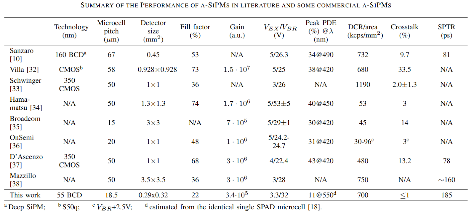
The AQUA research group at EPFL together with Global Foundries have published two new articles on 55 nm Bipolar-CMOS-DMOS (BCD) SPAD technology in the upcoming issues of IEEE Journal of Selected Topics in Quantum Electronics.
Engineering Breakdown Probability Profile for PDP and DCR Optimization in a SPAD Fabricated in a Standard 55 nm BCD Process


On Analog Silicon Photomultipliers in Standard 55-nm BCD Technology for LiDAR Applications


Product Videos: STMicro and Airy3D
Image Sensors World Go to the original article...
Low power, low noise 3D iToF 0.5 Mpix sensor
VD55G0 Consumer Global Shutter 0.4Mpix for Windows Hello Login
DepthIQ from AIRY3D
Canon Files Annual Report on Form 20-F for the Year Ended December 31, 2021
Black Phosphorus-based Intelligent Image Sensor
Image Sensors World Go to the original article...
Seokhyeong Lee, Ruoming Peng, Changming Wu & Mo Li from U-Dub have published an article in Nature Communications titled "Programmable black phosphorus image sensor for broadband optoelectronic edge computing".
Our blog had advertised a pre-print version of this work back in November 2021: https://image-sensors-world.blogspot.com/2021/11/black-phosphorus-vision-sensor.html.
Abstract: Image sensors with internal computing capability enable in-sensor computing that can significantly reduce the communication latency and power consumption for machine vision in distributed systems and robotics. Two-dimensional semiconductors have many advantages in realizing such intelligent vision sensors because of their tunable electrical and optical properties and amenability for heterogeneous integration. Here, we report a multifunctional infrared image sensor based on an array of black phosphorous programmable phototransistors (bP-PPT). By controlling the stored charges in the gate dielectric layers electrically and optically, the bP-PPT’s electrical conductance and photoresponsivity can be locally or remotely programmed with 5-bit precision to implement an in-sensor convolutional neural network (CNN). The sensor array can receive optical images transmitted over a broad spectral range in the infrared and perform inference computation to process and recognize the images with 92% accuracy. The demonstrated bP image sensor array can be scaled up to build a more complex vision-sensory neural network, which will find many promising applications for distributed and remote multispectral sensing.
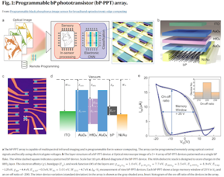
It is now peer reviewed and officially published as an open access paper: https://www.nature.com/articles/s41467-022-29171-1
Peer review report and authors' responses are also publicly available. In particular, it is interesting to see the response to some comments and about pixel non-uniformities, material stability during etching and longevity of the sensor prototype.
Some lightly edited excerpts from the reviews and authors responses below:
Reviewer: The optical image of the exfoliated flake clearly shows regions of varying thickness. How did the authors ensure each pixel is of the same thickness?
Authors: The mechanically exfoliated bP has several regions with different thicknesses. We fabricated all the pixels within a large region with uniform optical contrast, as outlined by the red dotted line, indicating uniform thickness. The thickness of the region is also confirmed with atomic force microscopy.
Reviewer: There is hardly any characterisation data provided for the material. How much of it is oxidised?
Authors: The oxidation of bP, it is indeed a concern. To mitigate that, we exfoliated and transferred bP in an Ar-filled glovebox. The device was immediately loaded into the atomic layer deposition (ALD) chamber to deposit the Al2O3 / HfO2 /Al2O3 (AHA) multilayers, which encapsulate the bP flake to prevent oxidation and degradation. This has been a practice reported in the literature, which generally leads to oxidation of only a few layers. Thanks to the 35 nm thick AHA encapsulation layer, our device shows long-term stability with persistent electrical and optical properties for more than 3 months after fabrication. We discuss that in the response to question 7. Furthermore, Raman spectroscopy shows no sign of Px Oy or Hx POy forming during the fabrication process. Thus, we expect that the oxidation of bP flake is no more than 3 layers (or 1.5 nm), which, if any, marginally affects the optical and electrical properties of the bP-PPT device.
Reviewer: Why did the authors focus only on the IR range when the black phosphorus can be even more broadband into the visible at the thickness used here?
Authors: The photoresponsivity of black phosphorus certainly extends to the visible band. We have
utilized both the visible and the IR range by engineering the device with the AHA stack: IR light to input images for optoelectronic in-sensor computing; visible light to optically program the device by activating the trapped charges and process the encoded images such as pattern recognition.
Reviewer: How long do the devices keep working in a stable manner?
Authors: We agree with the reviewer that more lifetime measurement data is important to ensure the
stability of the device’s operation. We have evaluated the performance of the bP-PPT devices over a long period of time (up to 3 months) ... the gate modulation, memory window, on-off ratio, and retention time of our devices remain consistent even 3 months after they were fabricated.
In today's day and age of Twitter, it's refreshing to see how science really progresses behind the scenes --- reviewers raising genuine concerns about a new technique; authors graciously accepting limitations and suggesting improvements and alternative ways forward.
Sony Cyber-shot P1 retro review
“NIKKOR – The Thousand and One Nights (Tale 81) has been released”
Hamamatsu Develops World’s First THz Image Intensifier
Image Sensors World Go to the original article...
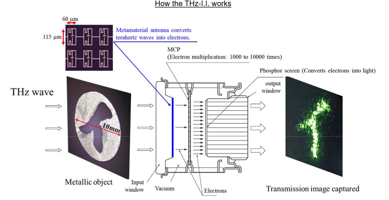
Hamamatsu Photonics has developed the world’s first terahertz image intensifier (THz image intensifier or simply THz-I.I.) by leveraging its imaging technology fostered over many years. This THz-I.I. has high resolution and fast response which allows for real-time imaging of terahertz wave (*) pulses transmitted through or reflected from target objects.
This THz-I.I. will be unveiled at “The 69th JSAP (Japan Society of Applied Physics) Spring Meeting” held at the Sagamihara Campus of Aoyama Gakuin University (in Sagamihara City, Kanagawa Prefecture, Japan) for 5 days from Tuesday, March 22 to Saturday, March 26.
Terahertz waves are electromagnetic waves near a frequency of 1 THz and have the properties of both light and radio waves.



Full press release: https://www.hamamatsu.com/content/dam/hamamatsu-photonics/sites/documents/01_HQ/01_news/01_news_2022/2022_03_14_en.pdf
Lensless camera for in vivo microscopy
Image Sensors World Go to the original article...
A team comprised of researchers from Rice University and Baylor College of Medicine in Houston, TX has published a Nature Biomedical Engineering article titled "In vivo lensless microscopy via a phase mask generating diffraction patterns with high-contrast contours."
Abstract: The simple and compact optics of lensless microscopes and the associated computational algorithms allow for large fields of view and the refocusing of the captured images. However, existing lensless techniques cannot accurately reconstruct the typical low-contrast images of optically dense biological tissue. Here we show that lensless imaging of tissue in vivo can be achieved via an optical phase mask designed to create a point spread function consisting of high-contrast contours with a broad spectrum of spatial frequencies. We built a prototype lensless microscope incorporating the ‘contour’ phase mask and used it to image calcium dynamics in the cortex of live mice (over a field of view of about 16 mm2) and in freely moving Hydra vulgaris, as well as microvasculature in the oral mucosa of volunteers. The low cost, small form factor and computational refocusing capability of in vivo lensless microscopy may open it up to clinical uses, especially for imaging difficult-to-reach areas of the body.


Link to full article (open access): https://www.nature.com/articles/s41551-022-00851-z
Press release: https://www.photonics.com/Articles/Lensless_Camera_Captures_Cellular-Level_3D_Details/a67869
Nikon Z9 review so far
Canon celebrates 19th consecutive year of No. 1 share of global interchangeable-lens digital camera market
Lensless Imaging with Fresnel Zone Plates
Image Sensors World Go to the original article...
Although the idea of Fresnel zone plates is not new and can be traced back several decades to X-ray imaging and perhaps to Fresnel's original paper from 1818*, there is renewed interest in this idea for visible light imaging due to the need for compact form-factor cameras.
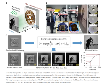
This 2020 article in the journal Light: Science and Applications by a team from Tsinghua University and MIT describes a lensless image sensor with a compressed-sensing style inverse reconstruction algorithm for high resolution color imaging.
Lensless imaging eliminates the need for geometric isomorphism between a scene and an image while allowing the construction of compact, lightweight imaging systems. However, a challenging inverse problem remains due to the low reconstructed signal-to-noise ratio. Current implementations require multiple masks or multiple shots to denoise the reconstruction. We propose single-shot lensless imaging with a Fresnel zone aperture and incoherent illumination. By using the Fresnel zone aperture to encode the incoherent rays in wavefront-like form, the captured pattern has the same form as the inline hologram. Since conventional backpropagation reconstruction is troubled by the twin-image problem, we show that the compressive sensing algorithm is effective in removing this twin-image artifact due to the sparsity in natural scenes. The reconstruction with a significantly improved signal-to-noise ratio from a single-shot image promotes a camera architecture that is flat and reliable in its structure and free of the need for strict calibration.


[Updated] 2022 International SPAD Sensor Workshop Final Program Available
Image Sensors World Go to the original article...
About ISSW 2022
Devices | Architectures | Applications
The International SPAD Sensor Workshop focuses on the study, modeling, design, fabrication, and characterization of SPAD sensors. The workshop welcomes all researchers, practitioners, and educators interested in SPADs, SPAD imagers, and associated applications, not only in imaging but also in other fields.
The third edition of the workshop will gather experts in all areas of SPADs and SPAD related applications using Internet virtual conference technology. The program is under development, expect three full days of with over 40 speakers from all over the world. This edition is sponsored by ams OSRAM.
Workshop website: https://issw2022.at/
Final program: https://issw2022.at/wp-content/uploads/2022/03/amsOSRAM_ISSW22_Program_3003.pdf


State of the Image Sensor Market
Image Sensors World Go to the original article...
Sigmaintell report on smartphone image sensors
According to Sigmaintell, the global mobile phone image sensor shipments in 2021 will be approximately 5.37B units, a YoY decrease of about 11.8%; among which, the global mobile phone image sensor shipments in 4Q21 will be about 1.37B units, a YoY decrease. About 25.3%. At the same time, it is estimated that the global mobile phone image sensor shipments will be about 5.50B in 2022, a year-on-year increase of about 2.5%. In 1H21, due to the long ramp-up cycle of ultra-high pixel production capacity and the squeeze of low-end pixel production capacity by other applications, there was a short-term structural imbalance and market price fluctuations rose. In 2H21, the production capacity of Samsung and Sony’s external foundries was released steadily and significantly, but the sales in the terminal market were lower than expected and the stocking plan was lowered again, resulting in an oversupply in the overall image sensor market.


Business Korea report about Samsung CIS foundry capacity expansion
Yole announces a new edition of its "Imaging for Security" Market report




Yole announces a new edition of its "Imaging for Automotive" market report


Strategy Analytics estimates USD15.1B global smartphone image sensor market in 2021
According to Strategy Analytics, the global smartphone Image sensor market in 2021 secured a total revenue of USD15.1B. Strategy Analytics finds that the smartphone image sensor market witnessed a revenue growth of more than 3% YoY in 2021. Sony Semiconductor Solutions topped with 45% revenue share followed by Samsung System LSI and OmniVision in 2021. The top 3 vendors captured nearly 83% revenue share in the global smartphone image sensor market in 2021. In terms of smartphone multi-camera application, Image sensors for Depth and Macro application reached 30 percent share while those for Ultrawide application exceeded 15% share.

ijiwei Insights predicts drop in mobile phone camera prices
In 2022, some manufacturers will reportedly reduce the price of mobile phone camera CIS several times. Currently, the cost down of phone camera CIS has penetrated into the camera chip products of 2MP, 5MP and 8MP. Among them, the unit price of 2MP and 5MP mobile phone camera CIS fell by about 20% and more than 30% year-on-year, respectively. [source]
New 3D Imaging Method for Microscopes
Image Sensors World Go to the original article...
New method for high resolution three dimension microscopic imaging being explored.
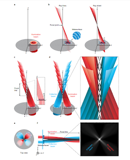
Metasurface-based bijective illumination collection imaging provides high-resolution tomography in three dimensions (Masoud Pahlevaninezhad, Yao-Wei Huang , Majid Pahlevani , Brett Bouma, Melissa J. Suter , Federico Capasso and Hamid Pahlevaninezhad )
Photonics Spectra article about Gigajot’s QIS Tech
Image Sensors World Go to the original article...
The March 2022 edition of Photonics Spectra magazine has an interesting article titled "Photon-Counting CMOS Sensors: Extend Frontiers in Scientific Imaging" by Dakota Robledo, Ph.D., senior image sensor scientist at Gigajot Technology.
While CMOS imagers have evolved significantly since the 1960s, photon-counting sensitivity has still requir