Sigma Updates on the Next Generation Foveon Sensor Development

Image Sensors World        Go to the original article...

Sigma publishes an official statement "Development status of the three-layer image sensor:"

Dear SIGMA customers,

First of all, thank you very much for your continued support and interest in our products.
SIGMA would like to share the development status of the three-layer image sensor as of February 2022 by the following.

The development of the three-layer image sensor is currently underway with the strong leadership of SIGMA’s headquarters in collaboration with research institutes in Japan. The stages of development can be roughly divided into the following:
  • Stage 1: Repeated design simulations of the new three-layer structure to confirm that it will function as intended.
  • Stage 2: Prototype evaluation using a small image sensor with the same pixel size as the product specifications but with a reduced total pixel count to verify the performance characteristics of the image sensor in practice.
  • Stage 3: Final prototype evaluation using a full-frame image sensor with the same specifications as the mass products including the AD converter etc…
We believe that these three stages are necessary in the development, and we are currently in the process of creating the prototype sensor for Stage 2.

Based on the evaluation results of the prototype sensor, we will decide whether to proceed to Stage 3 or to review the design data and re-prototype “Stage 2”. When we proceed to Stage 3, we will verify the mass-producibility of the sensor with research institutes and manufacturing vendors based on the evaluation results, and then make a final decision on whether or not to mass-produce the image sensor.

Although we have not yet reached the stage where we can announce a specific schedule for the mass production of the image sensor, we are determined to do our best to realize a camera that will truly please our customers who are waiting for it, as soon as possible.

Once again, I would like to thank all of you for your continued support of SIGMA.
We will continue to strive for technological development to meet your expectations and trust.

Kazuto Yamaki
Chief Executive Officer, SIGMA Corporation
Go to the original article...

Vision Sensor-Processor with In-Pixel Memory

Image Sensors World        Go to the original article...

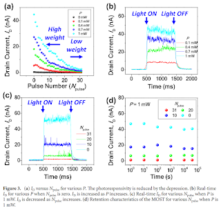
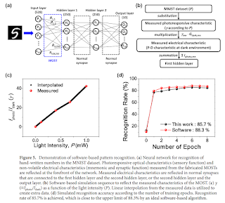
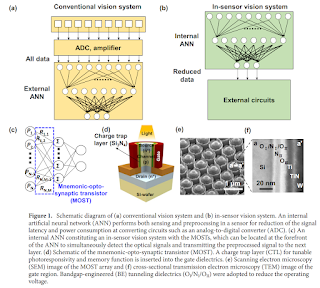
KAIST and Samsung foundry publish a Nature paper "Mnemonic-opto-synaptic transistor for in-sensor vision system" by Joon-Kyu Han, Young-Woo Chung, Jaeho Sim, Ji-Man Yu, Geon-Beom Lee, Sang-Hyeon Kim, and Yang-Kyu Choi.

"A mnemonic-opto-synaptic transistor (MOST) that has triple functions is demonstrated for an in-sensor vision system. It memorizes a photoresponsivity that corresponds to a synaptic weight as a memory cell, senses light as a photodetector, and performs weight updates as a synapse for machine vision with an artificial neural network (ANN). Herein the memory function added to a previous photodetecting device combined with a photodetector and a synapse provides a technical breakthrough for realizing in-sensor processing that is able to perform image sensing and signal processing in a sensor. A charge trap layer (CTL) was intercalated to gate dielectrics of a vertical pillar-shaped transistor for the memory function. Weight memorized in the CTL makes photoresponsivity tunable for real-time multiplication of the image with a memorized photoresponsivity matrix. Therefore, these multi-faceted features can allow in-sensor processing without external memory for the in-sensor vision system. In particular, the in-sensor vision system can enhance speed and energy efficiency compared to a conventional vision system due to the simultaneous preprocessing of massive data at sensor nodes prior to ANN nodes. Recognition of a simple pattern was demonstrated with full sets of the fabricated MOSTs. Furthermore, recognition of complex hand-written digits in the MNIST database was also demonstrated with software simulations."

Go to the original article...

High-Throughput SPAD Signal Processing

Image Sensors World        Go to the original article...

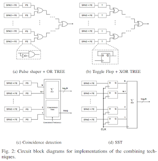
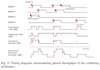
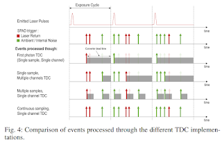
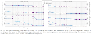
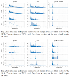
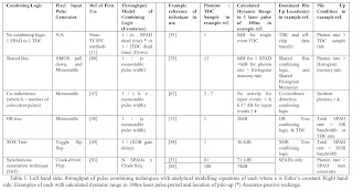
Edinburgh University and ST publish an open access IEEE JSSC paper "A High-Throughput Photon Processing Technique for Range Extension of SPAD-based LiDAR Receivers" by Sarrah M. Patanwala, Istvan Gyongy, Hanning Mai, Andreas Aßmann, Neale A. W. Dutton, Bruce R. Rae, and Robert K. Henderson.

"There has recently been a keen interest in developing LiDAR systems using SPAD sensors. This has led to a variety of implementations in pixel combining techniques and TDC architectures for such sensors. This paper presents a comparison of these approaches and demonstrates a technique capable of extending the range of LiDAR systems with improved resilience to background conditions. A LiDAR system emulator using a reconfigurable SPAD array and FPGA interface is used to compare these different techniques. A Monte Carlo simulation model leveraging synthetic 3D data is presented to visualize the sensor performance on realistic automotive LiDAR scenes."

Go to the original article...

dToF Tutorial from Edinburgh University and ST

Image Sensors World        Go to the original article...

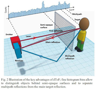
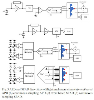
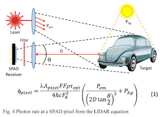
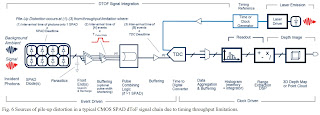
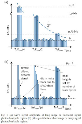
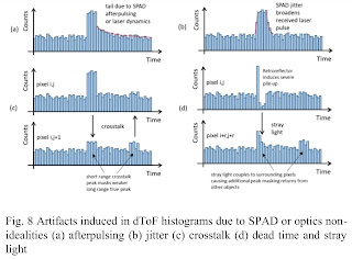
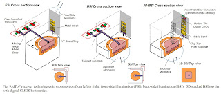
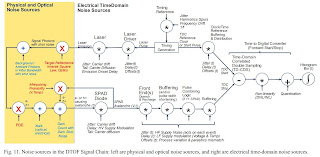
Edinburgh University publishes "Direct Time-of-Flight Single-Photon Imaging" by Istvan Gyongy, Neale A. W. Dutton, and Robert K. Henderson, also published by IEEE TED.

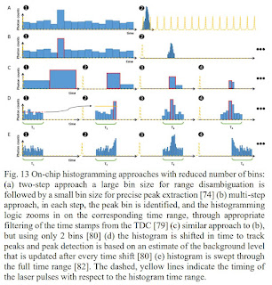
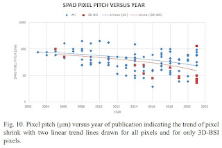
"This article provides a tutorial introduction to the direct Time-of-Flight (dToF) signal chain and typical artifacts introduced due to detector and processing electronic limitations. We outline the memory requirements of embedded histograms related to desired precision and detectability, which are often the limiting factor in the array resolution. A survey of integrated CMOS dToF arrays is provided highlighting future prospects to further scaling through process optimization or smart embedded processing."

Go to the original article...

Recent Videos: IIT Delhi, ADI, Omnivision, FLIR, Hamamatsu

Image Sensors World        Go to the original article...

IIT Delhi publishes a lecture "From light waves to images: Advancing Science with Pictures" by Kedar Khare:


Analog Devices publish a video on use case of its ADSD3100 platform based on Microsoft ToF sensor:


Omnivision publishes a promotional video for its 200MP OVB0B sensor with 0.61um pixels:


Teledyne FLIR demos the usefulness of thermal cameras in automatic emergency braking systems for cars:


Hamamatsu publishes a demo of its 8 x 128 pixel ToF sensor:


Go to the original article...

Himax Reports 2021 Results

Image Sensors World        Go to the original article...

GlobeNewswire: Himax updates on its imaging business in 2021:

"Himax is pleased to report that the company’s ultralow power AI image sensing total solution successfully entered into mass production in Q4 last year for a major tech name over a mainstream application. The company reached this major milestone just one year after it delivered the first samples, a remarkable achievement and an illustration of the robustness of AI solution. [I'd guess that this major customer is Amazon Ring and the product is video doorbell.]

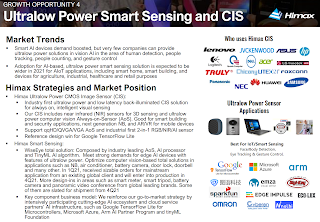
The company is highly encouraged by the early success it has seen with ultralow power AI image sensing business thus far after a leading customer adopted it for a mainstream application. Himax expects to see more design-wins awarded across a broad customer base and a high variety of applications leading to robust sales growth for this new high margin product line.

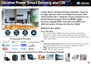
Himax’s ultralow power AI image sensing total solution incorporates its ultralow power CMOS image sensor, proprietary AI processor and CNN-based AI algorithm. As reported earlier, the sizable order for a top-tier name customer’s mainstream application successfully entered production in Q4 last year, marking another impressive milestone for company’s new AI business within just one year since its initial release. The company will give further details after the end customer’s official announcement. Himax has also made good progress on this mainstream application with other leading vendors where the number of design-in projects is increasing. In addition to the success story, the second application Himax expects to see significant volume is in automatic meter reading (AMR) where AI total solution has been widely adopted by numerous customers across a wide geographical area in China. Himax’s power-saving AI cameras, deployed over the existing installed base of traditional water meters, enable the water meter to automatically collect consumption data with AI operating locally on the edge. The device transmits only byte-sized metadata to the server for billing and in-time detection of abnormal consumption or leakage, eliminating the need for manual reading. The battery pack has a lifetime of over 5 years, greatly outperforming conventional AMR solutions which usually are in a bulky form with large battery packs and, without local AI capability, have to transmit massive image data to the cloud to perform meter reading.

The company is already seeing accelerated deployment of AI solutions to a wide range of applications, including notebook, home appliances, utility meter, automotive, battery-powered surveillance camera, panoramic video conferencing, and medical, among other things. Moreover, new design-in sockets are on the way as it looks to leverage the collaboration with leading cloud service partners, such as Microsoft Azure and Google TensorFlow, on their edge-to-cloud platform to drive further adoption on applications such as smart home, smart office, healthcare, agriculture, retail and factory automation. Last but not least, Himax is seeing numerous design-in activities of AI solution for endoscope, an area the company is extremely excited about that may represent an extraordinary game changer for the health examination industry. Himax will report more detail in due course. Himax is very encouraged by the traction this relatively new product line has generated in a short amount of time and expect to see increasing sales contribution through 2022 and beyond."
Go to the original article...

Intel Heritage in Image Sensors

Image Sensors World        Go to the original article...

It turns out that well before the Tower acquisition, in 90s, Intel already manufactured image sensors. Photobit designed it for Intel, Intel manufactured it, and then later Intel decided CMOS image sensors would be a commodity business and got out. Intel was Photobit’s first partner/customer. Intel Capital was an investor in Photobit for strategic purposes.

Go to the original article...

Yole Predicts that Sony and ST Will Capture 95% of SWIR Imagers Market

Image Sensors World        Go to the original article...

Yole Developpement believes that ST and Sony could disrupt the technological landscape with their SWIR imagers:

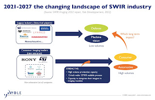
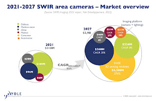
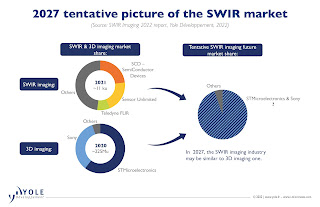
"In 2021, the SWIR industry’s leading players were SCD, Sensors Unlimited, and Teledyne FLIR, sharing more than 50% of the 11,000 units shipped in the year. These leaders are subsidiaries of leading defense companies that started developing SWIR technology with the support of governments for strategic purposes. They constitute the legacy side of the SWIR industry.

On the other side, STMicroelectronics and Sony, two leaders in the consumer imaging industry started being active players in SWIR with new technologies including quantum dots. Their entrance might be explained by the growing demand from consumer OEM for new integration designs such as under-display 3D sensing in smartphones. If SWIR imagers reach a low price point, shipments could skyrocket to hundreds of millions within a few years. The SWIR industry could emulate the current 3D imaging industry, where STMicroelectronics and Sony share nearly 95% of the 225 million shipments (2020 data)."
Go to the original article...

Peter Noble, Marvin White, and Northrop Grumman Win 2021 Emmi Awards

Image Sensors World        Go to the original article...

Peter Noble and Marvin White win 2021 Technology & Engineering Emmy Awards:
  • Correlated Double Sampling for Image Sensors
    • Marvin H. White
    • Northrop Grumman Mission Systems Group
  • Pioneering Development of an Image-Sensor Array with Buried-Photodiode Structure
    • Peter J. W. Noble

Go to the original article...

Peter Noble, Marvin White, and Northrop Grumman Win 2021 Emmy Awards

Image Sensors World        Go to the original article...

Peter Noble and Marvin White win 2021 Technology & Engineering Emmy Awards:
  • Correlated Double Sampling for Image Sensors
    • Marvin H. White
    • Northrop Grumman Mission Systems Group
  • Pioneering Development of an Image-Sensor Array with Buried-Photodiode Structure
    • Peter J. W. Noble

Go to the original article...

Sony "Sense the Wonder" Day

Image Sensors World        Go to the original article...

Sony publishes videos from its "Sense the Wonder" Day:

Go to the original article...

Omnivision Unveils 0.56um Pixel

Image Sensors World        Go to the original article...

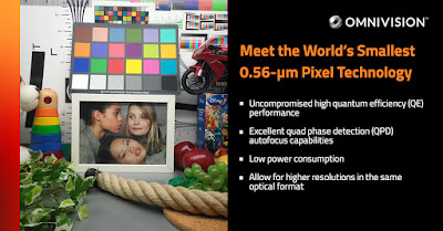
BusinessWire: OMNIVISION announces a major pixel technology breakthrough―the world’s smallest 0.56-µm pixel with high QE, excellent quad phase detection (QPD) autofocus and low power consumption. This ultra-small pixel technology will address the demand for high-resolution and small pixel pitch image sensors for multi-camera mobile devices.

With a pixel size now smaller than the wavelength of red light, OMNIVISION’s R&D team has validated that pixel shrink is no longer limited by the wavelength of light. The 0.56µm pixel design is enabled by a CIS-dedicated 28nm process node and 22nm logic process node at TSMC, with a new pixel transistor layout and 2x4 shared pixel architecture. The pixel is based on OMNIVISION’s PureCel Plus-S stacking technology, and deep photodiode technology is applied to embed the photodiode deeper into the silicon.

It takes great R&D innovation to advance pixel technology, especially at this level where we are going beyond the wavelength of light,” said Lindsay Grant, SVP of Process Engineering at OMNIVISION. “We have not compromised high performance with the smaller die size. In fact, we have demonstrated comparable QPD and QE performance to our 0.61µm pixel in the visible light range.
Grant adds, “OMNIVISION invests heavily in R&D and almost 50 percent of our employees comprise R&D engineers. As a global fabless semiconductor provider, we also work closely with our foundry partners, such as TSMC, to develop new process technology approaches that enable industry-leading innovation like this. This is a remarkable achievement, and I applaud our talented R&D team and our foundry partner for their ability to continuously lead the pixel shrink race.
We are pleased with the results of our deep collaboration with OMNIVISION in delivery of the world’s smallest 0.56-µm pixel using our industry-leading CIS technology,” said Sajiv Dalal, EVP of Business Management, TSMC North America. “TSMC strives to advance semiconductor manufacturing technologies and services to enable the most advanced, state-of-the-art CIS designs. We look forward to our continued partnership with OMNIVISION to help them achieve high performance, superior resolution, and low power consumption goals and accelerate innovation for their differentiated products.
The first 0.56µm pixel die will be implemented in 200MP image sensors for smartphones in Q2 2022, with samples targeted for Q3. Consumers can expect to see new smartphones that contain the world’s smallest pixel available on the market in early 2023.

Go to the original article...

Intel Gets into CIS Foundry Business through the Acquisition of Tower for $5.4B

Image Sensors World        Go to the original article...

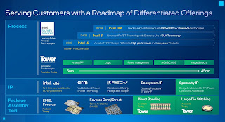
BusinessWire: Intel and Tower Semiconductor announce a definitive agreement under which Intel will acquire Tower for approximately $5.4 billion.

Tower’s specialty technology portfolio, geographic reach, deep customer relationships and services-first operations will help scale Intel’s foundry services and advance our goal of becoming a major provider of foundry capacity globally,” said Pat Gelsinger, Intel CEO. “This deal will enable Intel to offer a compelling breadth of leading-edge nodes and differentiated specialty technologies on mature nodes – unlocking new opportunities for existing and future customers in an era of unprecedented demand for semiconductors.

Tower owns 5 fabs directly and another 3 through a joint venture with Nuvoton. 6 of them manufacture image sensors, among other products. For some reason, Tower does not mention BSI processing joint venture with GPixel in China.


Update: Intel Investors Day presentation already shows CIS in the list of its foundry offerings:

Go to the original article...

OM System Olympus OM-1 review

Cameralabs        Go to the original article...

The Olympus OM-1 is the flagship mirrorless camera from OM System, sharing the same name as the classic film SLR celebrating its 50th anniversary. OM System gave me a brief chance to try out the OM-1 for my hands-on preview, so I can tell you all about what’s new and how it fits into the line-up. …

Go to the original article...

Hybrid ToF (hToF) Image Sensor Paper

Image Sensors World        Go to the original article...

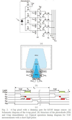
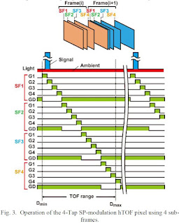
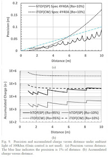
Shizuoka University publishes a IEEE Open JSSC paper "Hybrid Time-of-Flight Image Sensors for Middle-Range Outdoor Applications" by S. Kawahito, K. Yasutomi, and K. Mars.

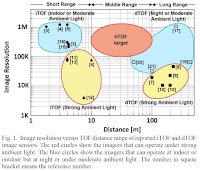
"This paper introduces a new series of time-of-flight (TOF) range image sensors that can be used for outdoor middle-range (10m to 100m) applications by employing a small duty-cycle modulated light pulse with a relatively high optical peak power. This set of TOF sensors is referred to here as a hybrid TOF (hTOF) image sensor. The hTOF image sensor is based on the indirect TOF measurement principle but simultaneously uses the direct TOF concept for coarse measurements. Compared to conventional indirect TOF image sensors for outdoor middle-range applications, the hTOF image sensor has a distinct advantage due to the reduction of capturing ambient light charge. To show the potential of the hTOF image sensor for outdoor middle-range operation, a model of estimating distance precision of hTOF image sensors is built and applied it by using possible sensor specifications to estimate the distance precision of the hTOF range camera in 10m, 20m and 40m measurements under the ambient-light condition of 100klux and its feasibility is discussed. In outdoor 10m-range measurements, the advantage of hTOF image sensors compared to the conventional indirect TOF image sensors is discussed by considering the amount of captured ambient-light charge in pixels."

Go to the original article...

Canon U.S.A., Inc. Is Successful Against eBay Counterfeiter

Newsroom | Canon Global        Go to the original article...

Go to the original article...

e2v Lecture on Image Sensor Performance Comparison

Image Sensors World        Go to the original article...

Vision Systems Design publishes a Youtube channel Vision Learning with quite a few interesting presentations. One of the recent presentations is 66min-long Teledyne e2v's "Understanding Image Sensor Performance - Interpret Key Parameters and Effective Comparison:"

Go to the original article...

Adaps dToF Paper

Image Sensors World        Go to the original article...

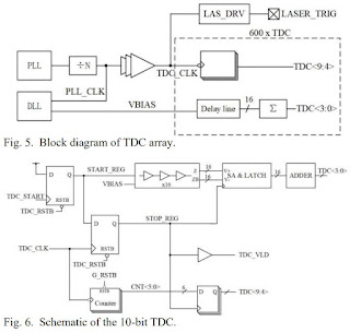
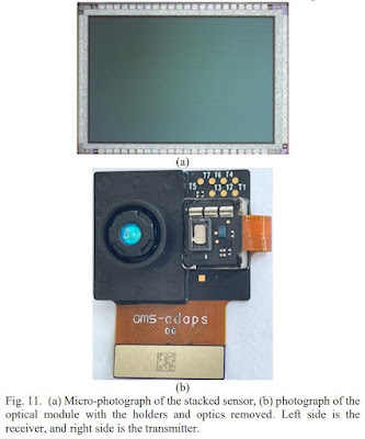
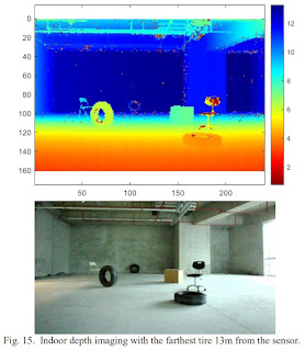
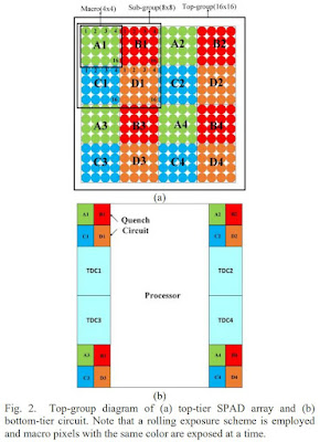
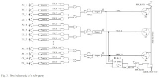
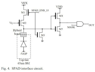
Shenzhen, China-based startup company Adaps Photonics publishes an open-access IEEE paper "A 240 x 160 3D Stacked SPAD dToF Image Sensor with Rolling Shutter and In Pixel Histogram for Mobile Devices" by Chao Zhang, Ning Zhang, Zhijie Ma, Letian Wang, Yu Qin, Jieyang Jia, and Kai Zang.

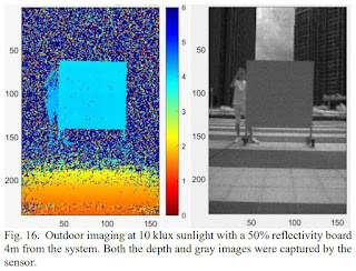
"A 240 x 160 single-photon avalanche diode (SPAD) sensor integrated with a 3D-stacked 65nm/65nm CMOS technology is reported for direct time-of-flight (dToF) 3D imaging in mobile devices. The top tier is occupied by backside illuminated SPADs with 16um pitch and 49.7% fill-factor. The SPADS consists of multiple 16x16 SPADs top groups, in which each of 8 x 8 SPADs sub-group shares a 10-bit, 97.65ps and 100ns range time-to-digital converter (TDC) in a quad-partition rolling shutter mode. During the exposure of each rolling stage, partial histogramming readout (PHR) approach is implemented to compress photon events to in-pixel histograms. Since the fine histograms is incomplete, for the first time we propose histogram distortion correction (HDC) algorithm to solve the linearity discontinuity at the coarse bin edges. With this algorithm, depth measurement up to 9.5m achieves an accuracy of 1cm and precision of 9mm in office lighting condition. Outdoor measurement with 10 klux sunlight achieves a maximum distance detection of 4m at 20 fps, using a VCSEL laser with the average power of 90 mW and peak power of 15 W."

Go to the original article...

Event Guided Depth Sensing

Image Sensors World        Go to the original article...

University of Zurich and ETH Zurich publish a paper "Event Guided Depth Sensing" by Manasi Muglikar, Diederik Paul Moeys, and Davide Scaramuzza.

"Active depth sensors like structured light, lidar, and time-of-flight systems sample the depth of the entire scene uniformly at a fixed scan rate. This leads to limited spatio-temporal resolution where redundant static information is over-sampled and precious motion information might be under-sampled. In this paper, we present an efficient bio-inspired event-camera-driven depth estimation algorithm. In our approach, we dynamically illuminate areas of interest densely, depending on the scene activity detected by the event camera, and sparsely illuminate areas in the field of view with no motion. The depth estimation is achieved by an event-based structured light system consisting of a laser point projector coupled with a second event-based sensor tuned to detect the reflection of the laser from the scene. We show the feasibility of our approach in a simulated autonomous driving scenario and real indoor sequences using our prototype. We show that, in natural scenes like autonomous driving and indoor environments, moving edges correspond to less than 10% of the scene on average. Thus our setup requires the sensor to scan only 10% of the scene, which could lead to almost 90% less power consumption by the illumination source. While we present the evaluation and proof-of-concept for an event-based structured-light system, the ideas presented here are applicable for a wide range of depth-sensing modalities like LIDAR, time-of-flight, and standard stereo. Video is available at https://www.youtube.com/watch?v=Rvv9IQLYjCQ"

Go to the original article...

Recent Videos: Ibeo, TI, Trioptics, Omnivision, ST, Gigajot

Image Sensors World        Go to the original article...

Ibeo publishes a video on LiDAR performance in fog and ways to improve it:

TI video shows an importance of clean power supply for image sensors:

Trioptics publishes its active alignment system video:


EETimes publishes an interview with Omnivision SVP Michael Wu about the company rebranding and latest products & partnership announcements:

ST publishes a video on choosing cover glass for its dToF proximity sensors (a longer version of this video is here):

Gigajot publishes its CTO Jiaju Ma presentation at Photonics Spectra conference:

Go to the original article...

Yole on 2021 Market Status

Image Sensors World        Go to the original article...

 Yole Developpement's Q4 2021 Quarterly CIS Market Monitor updates on the market status:

Go to the original article...

ON Semi Reports 45.2% Margins on CIS Products

Image Sensors World        Go to the original article...

SeekingAlpha publishes a transcript of Onsemi Q4 2021 earnings report. Few quotes:

"On the intelligent sensing front, our automotive imaging revenue grew by more than 20% quarter-over-quarter and approximately 40% year-over-year as we continue to see momentum in advanced safety with new design wins.

With consumers’ desire for additional safety features and an improved driving experience, we are seeing increased penetration of sensing in cars, including image sensors and ultrasonic sensing. At the same time, content per car is growing with each camera attached to one of our PMICs. We are also seeing accelerating demand for our imaging products for industrial and factory automation, in which revenue grew by approximately 10% quarter-over-quarter and 43% year-over-year. Industrial customers are investing in automation at an increased pace to improve efficiency and to reduce volatility in operations due to wage inflation and labor shortages, onshoring and social distancing mandates.

We have leveraged our experience in the automotive market to offer our industrial customers rugged, high resolution and high image quality sensors for the most demanding industrial applications. All of these execution vectors delivered a robust margin performance exceeding our target gross margin of 45% significantly ahead of schedule. This accelerated gross margin expansion was driven by a strong and accelerated execution in closing price-to-value discrepancy, cost reduction initiatives, a focused drive on ramping new products, a deliberate intent to shift more capacity to products for our strategic markets and operational efficiencies across our manufacturing footprint.

Revenue for Intelligent Sensing Group, or ISG, for the fourth quarter was $245.4 million, an increase of 18% year-over-year. GAAP gross margins for the fourth quarter was 45.1% and non-GAAP gross margin was 45.2%, a 370 basis point improvement quarter-over-quarter. The key contributors to our margin expansion have been favorable mix shift to higher margin and strategic products, elimination of price-to-value discrepancies in our portfolio and improved efficiencies in our manufacturing operations."

Go to the original article...

Galaxycore Stock Down by 17% in a Half Year after IPO

Image Sensors World        Go to the original article...

0033.com: On August 18, 2021, Lalaxycore was officially listed on the Science and Technology Innovation Board of the Shanghai Stock Exchange. Before the market, the total market value of Galaxycore once exceeded 100 billion yuan. On the first day of trading, Galaxycore  shares surged by 145.13%, and a total market value of 88.086 billion yuan.

As of January 28, 2022, Galaxycore's market value was 64.096 billion yuan, down by 17% within half a year of listing.

Zhao Lixin, the foun