Nikon releases the NIKKOR Z 600mm f/4 TC VR S, a fast, super-telephoto prime lens with a built-in 1.4x teleconverter for the Nikon Z mount system
Nikon releases the MC-N10 Remote Grip for the Nikon Z mount system
Canon’s EOS R3 wins highest-level Grand Award at DFA Design for Asia Awards 2022, the first full-frame mirrorless camera to receive the prize in the history of the DFA Awards
dToF Sensor with In-pixel Processing
Image Sensors World Go to the original article...
In a recent preprint (https://arxiv.org/pdf/2209.11772.pdf) Gyongy et al. describe a new 64x32 SPAD-based direct time-of-flight sensor with in-pixel histogramming and processing capability.


TechInsights Webinar on Hybrid Bonding Technologies Nov 15-16
Image Sensors World Go to the original article...
https://www.techinsights.com/webinar/hybrid-bonding-technologyThis webinar will:
- Examine different hybrid bonding approaches implemented in recent devices
- Discuss key players currently using this technology
- Look to the future of hybrid bonding, discussing potential wins – and pitfalls – to come.

Samsung announces 200MP ISOCELL HPX
Image Sensors World Go to the original article...
Samsung has announced the ISCOCELL HPX, a new 200MP sensor in China. This follows the June announcement of the ISOCELL HP3 200MP sensor. The ISOCELL HPX has 0.56-micron pixel size, which can reduce the camera module area by 20%, making the smartphone body thinner and smaller.
Furthermore, Samsung employed Advanced DTI (Deep Trench Isolation) technology, which not only separates each pixel individually, but also increases sensitivity to capture crisp and vivid images. Furthermore, the Super QPD autofocus solution enables ISOCELL HPX to have ultra-fast and ultra-precise autofocus.
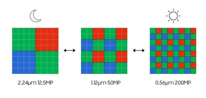
Tetra-Pixel technology in ISOCELL HPX sensor
Additionally, the Tetra pixel (16 pixels in one) technology is used in this new sensor that will give positive shooting experience in low light. With the help of this technology, the ISOCELL HPX is able to automatically switch between three different lighting modes depending on the available light: in a well-lit environment, the pixel size is maintained at 0.56 microns (μm), rendering 200 million pixels; in a low-light environment, the pixel is converted to 1.12 microns (μm), rendering 50 million pixels; and in a low-light environment, 16 pixels are combined to create a 2.24 micron (μm) 12.5 million pixel sensor.
According to Samsung, this technology enables ISOCELL HPX to deliver a positive shooting experience in low light and to reproduce sharp, sharp images as much as possible, even when the light source is constrained.
The ISOCELL HPX supports seamless dual HDR shooting in 4K and FHD modes and can capture 8K video at 30 fps. Depending on the shooting environment, Staggered HDR, according to Samsung, captures shadows and bright lights in a scene at three different exposures: low, medium, and high. Then it’ll combine all three exposure photos to produce HDR images and videos of the highest quality.
Additionally, it enables the sensor to render the image at over 4 trillion colours (14-bit colour depth), which is 64 times more than Samsung’s forerunner’s 68 billion colours (12-bit colour depth).
There’s no official wording from the firm regarding the availability. We should know in the coming weeks.
Another source covering this news: https://www.devicespecifications.com/en/news/17401435
VISION Stuttgart Videos
Image Sensors World Go to the original article...
Videos from the recent machine vision trade fair VISION Stuttgart are now available online.
Nikon releases the upgraded firmware version 3.00 for the Nikon Z 9 full-frame mirrorless camera
Atomos announces 8K video sensor
Image Sensors World Go to the original article...
Source: https://announcements.atomos.com/4207684IC Insights article on CMOS Image Sensors Market
Image Sensors World Go to the original article...
https://www.icinsights.com/news/bulletins/CMOS-Image-Sensors-Stall-In-Perfect-Storm-Of-2022/
CMOS Image Sensors Stall in ‘Perfect Storm’ of 2022

Nikon Photo Contest 2022-2023: Call for Entries
Nikon to exhibit a sample camera specially equipped with an image provenance function at Adobe MAX 2022
Canon RF 24mm f1.8 STM review
Canon’s activities lead to the removal of 1,171 listings from Amazon in Germany, Italy, Spain, the United Kingdom, France and The Netherlands
92 listings removed from Amazon in Canada, Mexico and the United States of America after Canon files infringement reports
Nikon COOLPIX 950 retro review
Videos du jour 2022-09-28: Teledyne, amsOSRAM, IEEE Sensors
Image Sensors World Go to the original article...
ESA-ESTEC Space & Scientific CMOS Image Sensors Workshop 2022
Image Sensors World Go to the original article...
Registration and other information: https://atpi.eventsair.com/workshop-on-cmos-image-sensors/registration-page/Site/Register
CNES, ESA, AIRBUS DEFENCE & SPACE, THALES ALENIA SPACE, SODERN are pleased to invite you to submit an abstract to the 7th “Space & Scientific CMOS Image Sensors” workshop to be held in ESA-ESTEC on November 22 nd and 23rd 2022 within the framework of the Optics and Optoelectronics COMET (Communities of Experts).
The aim of this workshop is to focus on CMOS image sensors for scientific and space applications.
Although this workshop is organized by actors of the Space Community, it is widely open to other professional imaging applications such as Machine vision, Medical, Advanced Driver Assistance Systems (ADAS), and Broadcast (UHDTV) that boost the development of new pixel and sensor architectures for high end applications.
Furthermore, we would like to invite Laboratories and Research Centres which develop Custom CMOS image sensors with advanced smart design on-chip to join this workshop.
Topics
Abstracts shall preferably address one or more of the following topics:
- Pixel design (low lag, linearity, FWC, MTF optimization, high quantum efficiency, large pitch pixels)
- Electrical design (low noise amplifiers, shutter, CDS, high speed architectures, TDI, HDR)
- On-chip ADC or TDC (in pixel, column, …)
- On-chip processing (smart sensors, multiple gains, summation, corrections)
- Electron multiplication, avalanche photodiodes
- Photon-counting, quanta image sensors
- Time resolving detectors (gated, time-correlated single-photon counting)
- Hyperspectral architectures
- Materials (thin film, optical layers, dopant, high-resistivity, amorphous Si)
- Processes (backside thinning, hybridization, 3D stacking, anti-reflection coating)
- Optical design (micro-lenses, trench isolation, filters)
- Large size devices (stitching, butting)
- CMOS image sensors with recent space heritage (in-flight performance)
- High speed interfaces
- Focal plane architectures
Tutorial Topics
Event-based sensors, SPADs
Industry exhibition
There are a limited number of small stands available for industry exhibitors. If you are interested in exhibiting at the Workshop, please contact the organisers.
Abstract submission
Please send a short abstract on one A4 page maximum in word or pdf format giving the title, the authors name and affiliation, and presenting the subject of your talk, to the organising committee (e-mail addresses are given hereafter).
Workshop format & official language
Oral presentation shall be requested for the workshop. The official language for the workshop is English.
Slide submission
After abstract acceptance notification, the author(s) will be requested to prepare their presentation in pdf or Powerpoint file format, to be presented at the workshop and to provide a copy to the organising committee with an authorization to make it available for all attendees, and on-line for the CCT members.
Calendar
13th September 2022 - Deadline for abstract submission
4th October 2022 - Author notification & preliminary programme
8th November 2022 - Final programme
22nd-23rd November 2022 - Workshop
Organising committee
| Alex MATERNE | CNES | alex.materne@cnes.fr | +33 5.61.28.15.44 |
| Nick NELMS | ESA | nick.nelms@esa.int | +31 71 565 8110 |
| Kyriaki MINOGLOU | ESA | kyriaki.minoglou@esa.int | +31 71 565 3797 |
| Serena RIZZOLO | Airbus Defence & Space | Serena.rizzolo@airbus.com | +33 5.62.19.62.77 |
| Stéphane DEMIGUEL | Thalès Alenia Space | stephane.demiguel@thalesaleniaspace.com | +33 4.92.92.61.89 |
| Aurelien VRIET | SODERN | aurelien.vriet@sodern.fr | +33 1.45.95.70.00 |
Canon Wins U.S. Trademark Infringement Lawsuit Against Counterfeiters
Canon Utsunomiya Office to install new manufacturing facilities, strengthen manufacturing capacity for semiconductor lithography systems
Calumino raises $10.3m for AI-based thermal sensing
Image Sensors World Go to the original article...
From Geospatial World: https://www.geospatialworld.net/news/calumino-10-3mn-funding-ai-thermal-sensing-platform/
Calumino, the developer and manufacturer of a proprietary next-generation thermal sensor technology and AI, today announced its $10.3M USD Series A funding. The funding round is led by Celesta Capital and Taronga Ventures, with additional participation from Egis Technology and others. Calumino’s innovation offers the first-ever intelligent sensing platform, which is an aggregator of new and valuable data points on human presence, activity, hazards, and the environment.
As the world’s first thermal sensor to combine A.I. with high performance image sensing, privacy protection, and affordability, Calumino’s platform enables new benefits for a broad range of applications. This includes smart building management, pest control, safety and security, healthcare, and more. The Calumino thermal sensor has been natively designed with a sufficiently low resolution to protect an individual’s privacy, which in turn fills the current market gap between intrusive IP cameras and low performance motion sensors.
Sensing temperatures rather than light, the Calumino thermal sensor maps environments, assets, and individuals and has the ability to detect human presence, activity, and posture. It can also differentiate humans from animals and detect hazardous hotspots, fires, water leaks, and other anomalies. This unique data is essential for saving energy, increasing business operation efficiencies, increasing security and safety, improving life quality, and saving lives.
The Series A funding follows the successful commercialization of Calumino’s technology in the areas of commercial building management and pest control. Most recently, the company has entered the Japanese market with a Mitsubishi Electric subsidiary as a strategic partner, launching its innovative pest control product “Pescle” based upon the Calumino thermal sensor + AI.
“We are incredibly excited about this partnership and plan to roll this product out globally with our partners,” said Marek Steffanson, Founder and CEO of Calumino. “No other technology can differentiate between humans and rodents reliably, in darkness, affordably, intelligently, and with very low data bandwidth – but this application is just the beginning. Our technology is creating an entirely new space in the market and we are incredibly grateful to our investors for their support as we continue to scale production and enable the next generation of intelligent sensing to solve important problems.”
With its Series A proceeds, Calumino plans to expand existing applications and create new use cases. The team also plans to further invest in research and development, as well as expand its global team including new offices in Europe, Taiwan, Japan, and the United States.
“Calumino’s unique technology is helping to drive the proliferation of IoT – the intelligence of things – and enabling for the first time intelligent thermal imaging that is cost-effective, privacy-protecting, and scalable to mass markets,” said Nicholas Brathwaite, Founding Managing Partner of Celesta Capital. “Celesta is excited to offer our financial and intellectual capital support to help Calumino pursue their bold ambitions in becoming the ultimate IoT technology.”
“Calumino’s affordable and intelligent technology is changing the standard of how we live, work and play in real assets. The unique data and insights that Calumino is able to provide will enable asset owners to create safe, secure, and healthy environments using market-leading technology”, said Sven Sylvester, Investment Director at Taronga Ventures.
Prophesee closes EUR 50 million Series C
Image Sensors World Go to the original article...
Prophesee closes €50M C Series round with new investment from Prosperity7 to drive commercialization of revolutionary neuromorphic vision technology;
Becomes EU’s most well-funded fabless semiconductor startup
Link: https://www.prophesee.ai/2022/09/22/prophesee-closes-50million-fundraising-round/
PARIS, September 22, 2022 – Prophesee, the inventor of the world’s most advanced neuromorphic vision systems, today announced the completion of its Series C round of funding with the addition of a new investment from Prosperity7 ventures. The round now totals €50m, including backing from initial Series C investors Sinovation Ventures and Xiaomi. They join an already strong group of international investors from North America, Europe and Japan that includes Intel Capital, Robert Bosch Venture Capital, 360 Capital, iBionext, and the European Investment Bank.
With the investment round, Prophesee becomes EU’s most well-funded fabless semiconductor startup, having raised a total of €127M since its founding in 2014.
Prosperity7 Ventures, the diversified growth global fund of Aramco Ventures – a subsidiary of Saudi Aramco, is on constant search for transformative technologies and innovative business models. Its mission is to invest in the disruptive technologies with the potential to create next-generation technology leaders and bring prosperity on a vast scale. It currently has $1B under management and holds diversified investments across various sectors, including in deep tech and bio-science companies.
“Gaining the support of such a substantial investor as Prosperity7 adds another globally-focused backer that has a long-term vision and understanding of the requirements to achieve success with a deep tech semiconductor investment. Their support is a testament to the progress achieved and the potential that lies ahead for Prophesee. We appreciate the rigor which they, and all our investors, have used in evaluating our technology and business model and are confident their commitment to a long-term relationship will be mutually beneficial,” said Luca Verre, co-founder and CEO of Prophesee.
The round builds further momentum for Prophesee in accelerating the development and commercialization of its next generation hardware and software products, as well as position it to address new and emerging market opportunities and further scale the company. The support from its investors strengthens its ability to develop business opportunities across key ecosystems in semiconductors, industrial, robotics, IoT and mobile devices.
Event cameras address the challenges of applying computer vision in innovative ways
“Prophesee is leading the development of a very unique solution that has the potential to revolutionize and transform the way motion is captured and processed.” noted Aysar Tayeb, the Executive Managing Director at Prosperity7. “The company has established itself as a clear leader in applying neuromorphic methods to computer vision with its revolutionary event-based Metavision® sensing and processing approach. With its fundamentally differentiated AI-driven sensor solution, its demonstrated track record with global leaders such as Sony, and its fast-growing ecosystem of more than 5,000 developers using its technology, we believe Prophesee is well-positioned to enable paradigm-shift innovation that brings new levels of safety, efficiency and sustainability to various market segments, including smartphones, automotive, AR/VR and industrial automation.” Aysar further emphasized “Prophesee and its unique team hit the criteria we are constantly searching for in startup companies with truly disruptive, life-changing technologies.”
Prophesee’s approach to enabling machines to see is a fundamental shift from traditional camera methods and aligns directly with the increasing need for more efficient ways to capture and process the dramatic increase in the volume of video input. By utilizing neuromorphic techniques to mimic the way that human brain and eye work, Prophesee’s event-based Metavision technology significantly reduces the amount of data needed to capture information. Among the benefits of the sensor and AI technology are ultra-low latency, robustness to challenging lighting conditions, energy efficiency, and low data rate. This makes it well-suited for a broad range of applications in industrial automation, IoT, consumer electronics that require real-time video data analysis while operating under demanding power consumption, size and lighting requirements.
Prophesee has gained market traction with key partners around the world who are incorporating its technology into sophisticated vision systems for uses cases in smartphones, AR/VR headsets, factory automation and maintenance, science and health research. Its partnership with Sony has resulted in a next generation HD vision sensor that combines Sony’s CMOS image sensor technology with Prophesee’s unique event-based Metavision® sensing technology. It has established commercial partnership with leading machine vision suppliers such as Lucid, Framos, Imago and Century Arks, and its open-source model for accessing its software and development tools has enabled a fast-growing community of 5,000+ developers using the technology in new and innovative ways.
Canon SELPHY CP1500 review
“NIKKOR – The Thousand and One Nights (Tale 83) has been released”
TechInsights on new iPhone 14 camera module


Canon’s enforcement of its intellectual property right leads to the removal of toner cartridges, including cartridges sold by flagship shop of Goodream as “GOODREAM” brand, from Tmall
Arducam’s New ToF Camera Module for Embedded Applications
Image Sensors World Go to the original article...
- Real-time point cloud and depth map.
- Resolution: 240x180@30fps on RPI4/CM4
- Up to 4M measuring distance
- Onboard 940nm laser for both indoor & outdoor uses, no external light source needed.
- V4L2-based video kernel device
- C/C++/Python SDK for userland depth map output and example source code
- ROS ready
- 38 x 38mm board size


Kickstarter link: https://www.kickstarter.com/projects/arducam/time-of-flight-tof-camera-for-raspberry-pi
Alpsentek "hybrid" vision sensor for HDR imaging
Image Sensors World Go to the original article...
From the VISION 2022 exhibition in Stuttgart:
AlpsenTek® launches the ALPIX-Eiger™, a fusion vision sensor for high-end imaging
AlpsenTek®, a leading developer of fusion vision sensors, announced the launch of the ALPIX-Eiger™ fusion vision sensor chip, specifically designed for high-end imaging applications. Using the original patented Hybrid Vision™ fusion vision technology, ALPIX-Eiger™ enables the fusion of image sensing and event sensing at the pixel level, making the simultaneous output of both image and event streams possible.
ALPIX-Eiger ™ is a patented chip architecture and pixel design with advanced 3D stacking and BSI back-illuminated/backlight technology. With a pixel size of just 1.89µm×1.89µm and a resolution of 8.0 megapixels, it is the smallest pixel size and highest resolution image sensor with event-aware capabilities in the industry. It offers broad application capabilities to small-sized smart devices, such as mobile phones and motion cameras.
High performance
The ALPIX-Eiger™ not only maintains the advantages of image sensors, ensuring full image quality and rich image details but also facilitates event sensing through the patented design of digital-analog mixed signal processing in pixels. This technology allows single pixel to work independently to detect light changes. Having a response speed of microseconds, high frame rate (equivalent to 5000fps), high dynamic range (110dB), low data redundancy and other characteristics helps the image sensor obtain more information and enhances image quality. Compared with previous event camera solutions, the event stream output by ALPIX-Eiger™ carries color information, which aids color reconstruction of the image and achieves better quality photo and video capabilities.
Wide Applications
In practical applications, intelligent imaging devices equipped with ALPIX-Eiger™ chips can achieve high-end functions such as de-blurring, high frame rate, and super-resolution to facilitate the development of more visual applications. The HDR performance and instantaneous response of the ALPIX-Eiger™ also allow the device to obtain better imaging results at night in scenarios with extreme light and dark contrasts.

Other recent posts about Alpsentek:
https://image-sensors-world.blogspot.com/2022/06/alpsentek-vision-sensor-startup-raises.html
https://image-sensors-world.blogspot.com/2021/11/interview-with-ceo-of-ruisi-zhixin.html
http://image-sensors-world.blogspot.com/2021/10/chinese-startup-ruisizhixin-develops.html
ST’s new ToF sensor uses a metalens
Image Sensors World Go to the original article...
Recent EE Journal article suggests that the 2nd generation time-of-flight proximity sensor from STMicro uses metalenses designed by Metalenz, a Harvard spinoff.
Original article here: https://www.eejournal.com/article/time-of-flight-sensors-trilobites-and-tunable-optics-what-an-unlikely-combo/
Some excerpts below:
Time of Flight Sensors, Trilobites, and Tunable Optics – What an Unlikely Combo!
STMicroelectronics has added a new member to its line of VL53 FlightSense TOF (time of flight) distance/ranging sensors, but this new sensor takes a radical departure from the previous generation by replacing a conventional lensing system with metalenses, developed in conjunction with a startup company called Metalenz and based on technology originally developed in a Harvard University metamaterial lab. According to Metalenz, this is the first commercial product to incorporate its metalens technology.

The resulting TOF sensor can achieve more than double the range – as much as 4m in indoor settings – or it can operate at half the power consumption relative to ST’s previous generation of VL53 TOF sensors. The expanded range and reduced power consumption arise from a combination of a more efficient VCSEL driver circuit and the improved light-gathering ability of the metalens covering the SPAD array. ST’s announcement did not specify a minimum target distance for the VL53L8 sensor, but its predecessor, the VL53L5CX sensor, has a minimum ranging distance of 2cm and an apparent resolution of 1mm, with ±15mm accuracy in the 20-200mm range and 4-11% in the 201-4000mm range, depending on ambient lighting.
Like the earlier VL53L5CX sensor, the new VL53L8 sensor can determine distance to a target or multiple targets simultaneously using either 16 zones at 60Hz or 64 zones at 15Hz, as observed through a 43.5° x 43.5° square field of view. An integrated microcontroller in the TOF sensor delivers range-to-target information directly over an I2C or SPI serial interface and can generate interrupts to wake a host processor when each distance reading is made. Even with all it packs inside, this is a physically tiny sensor, measuring 6.4 x 3.0 x 1.75 mm. It’s supplied as a single, factory-aligned, reflowable component so you can drop it into a variety of products, even small portable ones.
A recent press-release from Metalenz confirms that they have indeed partnered with ST on the new VL53L8 proximity sensor.
Press release: https://www.metalenz.com/the-worlds-first-metasurfaces-have-arrived-on-the-market/
Boston, MA and Geneva, Switzerland – June 9, 2022 – Metalenz, the first company to commercialize meta-optics, and STMicroelectronics (NYSE: STM), a global semiconductor leader serving customers across the spectrum of electronics applications, today announce that ST’s currently released VL53L8 direct Time-of-Flight (dToF) sensor is the highly anticipated market debut of the meta-optics devices developed through their partnership, which was disclosed in June 2021.
Metalenz’s Harvard-born, meta-optics technology can replace existing complex and multi-element lenses and provide additional functionality with a single meta-optic embedded in time-of-flight (ToF) modules from ST, the leading company in supplying 3D sensing modules. The introduction of Metalenz technology in these modules brings performance, power, size, and cost advantages to a multitude of consumer, automotive, and industrial applications. This marks the first time metasurface technology is commercially available and being used in consumer devices.
Unlike traditional molded and curved lenses, Metalenz’s novel optics are completely planar. Planar metasurface optics are now being manufactured on silicon wafers alongside electronics in ST’s semiconductor front-end fabs for the first time. The meta-optics collect more light, provide multiple functions in a single layer, and enable new forms of sensing in smartphones and other devices, while taking up less space. Metalenz’s flat-lens technology replaces certain existing optics in ST’s FlightSense™ ToF modules, which serve applications such as smartphones, drones, robots, and vehicles. In these, ST has sold more than 1.7 billion units to date.
“More than a decade of foundational research has brought us to this point. Market deployment of our meta-optics makes this the first metasurface technology to become commercially available,” said Rob Devlin, co-founder and CEO of Metalenz. “ST’s technology, manufacturing expertise, and global reach allow us to impact millions of consumers. We have multiple wins that mark the first application of our platform technology and we are now designing entire systems around its unique functionality. Our meta-optics enable exciting new markets and new sensing capabilities in mobile form factors and at a competitive price.”
