Weekly Updates

Image Sensors World        Go to the original article...


Nikon Designs Sensor That Has Both a Global and Rolling Shutter

Nikon has filed a patent for a new type of sensor that would allow it to perform both a rolling and global shutter operation. It’s not the first time the company has proposed such a design, but it expands on the use case of a previous filing. ...


Programmable Black Phosphorus Image Sensor For Broadband Optoelectronic Edge Computing

Image sensors with internal computing capability enable in-sensor computing that can significantly reduce the communication latency and power consumption for machine vision in distributed systems and robotics. Two-dimensional semiconductors have many advantages in realizing such intelligent vision sensors because of their tunable electrical and optical properties and amenability for heterogeneous integration. ...


Samsung Quietly Unveils The Galaxy A73 5G, Its First Mid-Range Phone with a 108MP Camera


In 2020, Samsung introduced the Galaxy S20 Ultra to the market, and its main selling point was an all-new 108MP rear sensor. The camera experience was a little rough around the edges, but it improved a bit in the Note20 Ultra and the S21 Ultra and even more in this year's S22 Ultra. Up to this point, those 108MP cameras had remained a selling point of the Ultra range, as other S devices didn't get them. But now Samsung has unveiled the Galaxy A73 5G, the phone that's breaking that trend for the first time. ...


Intel Investing $100 Million in Semiconductor Education

"Our goal is to bring these programs and opportunities to a variety of two-year and four-year colleges, universities, and technical programs, because it is critical that we expand and diversify STEM education." An additional $50 million will be matched by the U.S. National Science Foundation (NSF), which will be asking for proposals from educators for a curriculum that aims to improve STEM education at two-year colleges and four-year universities. ...


The Neon Shortage Is a Bad Sign: Russia's war against Ukraine has ramifications for the chips that power all sorts of tech

Neon, a colorless and odorless gas, is typically not as exciting as it sounds, but this unassuming molecule happens to play a critical role in making the tech we use every day. For years, this neon has also mostly come from Ukraine, where just two companies purify enough to produce devices for much of the world, usually with little issue. At least, they did until Russia invaded. ...


Patent Tip, Based on a True Story: Contour IP Holdings, LLC v. GoPro

"Patent Owners should avoid describing and claiming the advance over the prior art in purely functional terms, in a result-oriented way that amounts to encompassing the abstract solution no matter how implemented. Instead, Patent Owners should describe and claim technical details for tangible components in the claimed system, showing that such components are technologically innovative and not generic. For computer-implemented inventions, this may include a specific set of computer digital structures to solve a specific computer problem." ...

Go to the original article...

In the News: Week of March 14, 2022

Image Sensors World        Go to the original article...

China COVID spike may affect image sensor supply

Digitimes Asia reports: "A spike in COVID-19 cases in Hong Kong and other Chinese cities is disrupting handset CMOS image sensor (CIS) shipments, as well as deliveries of related modules and other devices, according to industry sources." [source]


Luminous Computing Appoints Michael Hochberg as President

EETimes reports: "Luminous Computing, a machine learning systems company based in California, announced today the appointment of Michael Hochberg as president. Hochberg will lead engineering and operations at Luminous to develop what the company claims is the world’s most powerful artificial intelligence (AI) supercomputer to market, driven by silicon photonics technology. [source]


James Webb Telescope Camera Outperforming Expectations  

NASA reports: "On March 11, the Webb team completed the stage of alignment known as “fine phasing.” At this key stage in the commissioning of Webb’s Optical Telescope Element, every optical parameter that has been checked and tested is performing at, or above, expectations. The team also found no critical issues and no measurable contamination or blockages to Webb’s optical path. The observatory is able to successfully gather light from distant objects and deliver it to its instruments without issue." [source]

DSLR Confusion

Poking fun at a recent NYPost shopping guide on "Best DSLRs" list that contains mirrorless cameras, PetaPixel reports: "People Have No Idea What a DSLR Actually Is" [source] 

If you have any interesting news articles and other tidbits worth sharing on this blog please email ingle dot atul at ieee dot org.

Go to the original article...

trinamiX Face Authentication Tech Receives IIFAA Certificate

Image Sensors World        Go to the original article...

trinamiX Face Authentication fulfills the biometric security requirements defined by the International Internet Finance Authentication Alliance (IIFAA). After recently announcing the fulfilment of the FIDO Alliance and Android Biometric Security standards, the German tech company is now topping it off with their newest certification. trinamiX GmbH, a subsidiary of BASF SE, has thereby proven to be suited for integration in digital payment processes with particularly high security demands. Their solution is the first to pass these tests while the hardware is invisibly mounted behind OLED. IIFAA’s standard is adhered to by leading players in the FinTech industry and has the widest market coverage in China.

trinamiX Face Authentication became the world’s first to pass all these tests and to provide “financial-level security”2 while all hardware was integrated behind a full-screen display. “We’ve finally received living proof of our capability to raise the bar of biometric security,” Stefan Metz, Director 3D Imaging Business at trinamiX, stated. “Our solution can mean a breakthrough to the world of digital payment, allowing users to better trust in and benefit from digital financial services.” The innovative strength of this solution unveils itself through a closer look into the underlying technology: trinamiX Face Authentication introduces a one-of-a-kind liveness check to the authentication process in order to tell whether the object in front of the camera is an actual human-being. In addition to checking the presented face for three-dimensional depth, it reliably detects skin versus other materials. Thanks to skin detection, not even a hyperrealistic replica of a user’s face can trick the system – while common biometric authentication solutions are still prone to these fraud attempts.

The latest test result of trinamiX Face Authentication, issued by IIFAA’s testing agency, certifies that the solution complies with the IIFAA Biometric Face Security Test Requirement, which is an established authentication standard for digital financial services.

Full article: https://trinamixsensing.com/news-events/press/trinamix-face-authentication-behind-oled-earns-international-biometric-security-certificate-by-iifaa/

Go to the original article...

SmartSens 50MP Ultra-High-Resolution Image Sensor

Image Sensors World        Go to the original article...

SmartSens has launched an ultra high resolution image sensor based on a 22nm process. SC550XS is their first 50MP ultra-high resolution image sensor with a 1.0μm pixel size. The new product adopts the advanced 22nm HKMG Stack process as well as SmartSens’ multiple proprietary technologies, including SmartClarity®-2 technology, SFCPixel® technology and PixGain HDR® technology to enable excellent imaging performance. In addition, it can achieve 100% all pixel all direction auto focus coverage via AllPix ADAF® technology and is equipped with MIPI C-PHY 3.0Gsps high-speed data transmission interface. The product is designed to address the requirements of flagship smartphone main camera in terms of night vision full-color imaging, high dynamic range, and low power consumption.


Full press release: https://www.smartsenstech.com/en/page?id=179

Go to the original article...

Low Power Edge-AI Vision Sensor

Image Sensors World        Go to the original article...

Another interesting article from the upcoming tinyML conference. This one is titled "P2M: A Processing-in-Pixel-in-Memory Paradigm for Resource-Constrained TinyML Applications" and is work done by a team from University of Southern California.

The demand to process vast amounts of data generated from state-of-the-art high resolution cameras has motivated novel energy-efficient on-device AI solutions. Visual data in such cameras are usually captured in the form of analog voltages by a sensor pixel array, and then converted to the digital domain for subsequent AI processing using analog-to-digital converters (ADC). Recent research has tried to take advantage of massively parallel low-power analog/digital computing in the form of near- and in-sensor processing, in which the AI computation is performed partly in the periphery of the pixel array and partly in a separate on-board CPU/accelerator. Unfortunately, high-resolution input images still need to be streamed between the camera and the AI processing unit, frame by frame, causing energy, bandwidth, and security bottlenecks. To mitigate this problem, we propose a novel Processing-in-Pixel-in-memory (P2M) paradigm, that customizes the pixel array by adding support for analog multi-channel, multi-bit convolution and ReLU (Rectified Linear Units). Our solution includes a holistic algorithm-circuit co-design approach and the resulting P2M paradigm can be used as a drop-in replacement for embedding memory-intensive first few layers of convolutional neural network (CNN) models within foundry-manufacturable CMOS image sensor platforms. Our experimental results indicate that P2M reduces data transfer bandwidth from sensors and analog to digital conversions by ~21x, and the energy-delay product (EDP) incurred in processing a MobileNetV2 model on a TinyML use case for visual wake words dataset (VWW) by up to ~11x compared to standard near-processing or in-sensor implementations, without any significant drop in test accuracy.


arXiv preprint: https://arxiv.org/pdf/2203.04737.pdf

tinyML conference information: https://www.tinyml.org/event/summit-2022/

Go to the original article...

A Curious Observation about 1-bit Quanta Image Sensors Explained

Image Sensors World        Go to the original article...

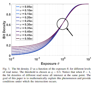
Dr. Stanley Chan (Purdue University) has a preprint out titled "On the Insensitivity of Bit Density to Read Noise in One-bit Quanta Image Sensors" on arXiv. This paper presents a rigorous theoretical analysis of an intuitive but curious observation that was first made in the paper by E. Fossum titled "Analog read noise and quantizer threshold estimation from Quanta Image Sensor Bit Density."

Why is the quanta image sensor bit density insensitive to read noise at high enough exposure values?

The one-bit quanta image sensor is a photon-counting device that produces binary measurements where each bit represents the presence or absence of a photon. In the presence of read noise, the sensor quantizes the analog voltage into the binary bits using a threshold value q. The average number of ones in the bitstream is known as the bit-density and is often the sufficient statistics for signal estimation. An intriguing phenomenon is observed when the quanta exposure is at unity and the threshold is q=0.5. The bit-density demonstrates a complete insensitivity as long as the read noise level does not exceeds a certain limit. In other words, the bit density stays at a constant independent of the amount of read noise. This paper provides a mathematical explanation of the phenomenon by deriving conditions under which the phenomenon happens. It was found that the insensitivity holds when some forms of the symmetry of the underlying Poisson-Gaussian distribution holds.


The paper concludes:

The insensitivity of the bit density of a 1-bit quanta image sensor is analyzed. It was found that for a quanta exposure θ = 1 and an analog voltage threshold q = 0.5, the bit density D is nearly a constant whenever the read noise satisfies the condition σ ≤ 0.4419. The proof is derived by exploiting the symmetry of the Gaussian cumulative distribution function, and the symmetry of the Poisson probability mass function at the threshold k = 0.5. An approximation scheme is introduced to provide a simplified estimate where σ ≤ 1/√2π = 0.4. In general, the analysis shows that the insensitivity of the bit density is more of a (very) special case of the 1-bit quantized Poisson-Gaussian statistics. Insensitivity can be observed when the quanta exposure θ is an integer and the threshold is q = θ−0.5. As soon as the pair (θ, q) deviates from this configuration, the insensitivity will no longer appear.

Complete article can be downloaded here: https://arxiv.org/pdf/2203.06086

An early-access version of Eric's paper is available here: https://ieeexplore.ieee.org/document/9729893

Go to the original article...

High Resolution MEMS LiDAR Paper in Nature Magazine

Image Sensors World        Go to the original article...

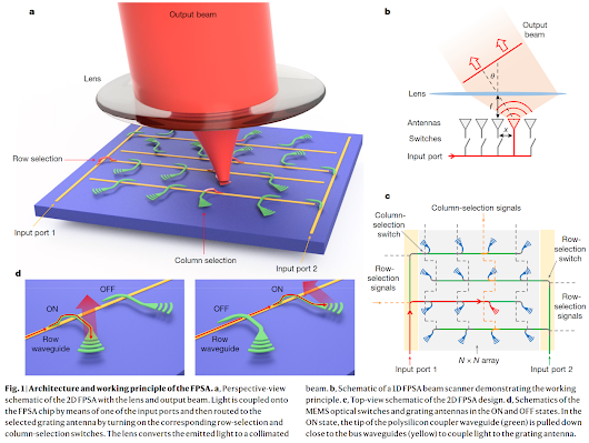
Researches from the Integrated Photonics Lab at UC-Berkeley recently published a paper titled "A large-scale microelectromechanical-systems-based silicon photonics LiDAR" proposing a CMOS-compatible high-resolution scanning MEMS LiDAR system.

Three-dimensional (3D) imaging sensors allow machines to perceive, map and interact with the surrounding world. The size of light detection and ranging (LiDAR) devices is often limited by mechanical scanners. Focal plane array-based 3D sensors are promising candidates for solid-state LiDARs because they allow electronic scanning without mechanical moving parts. However, their resolutions have been limited to 512 pixels or smaller. In this paper, we report on a 16,384-pixel LiDAR with a wide field of view (FoV, 70° × 70°), a fine addressing resolution (0.6° × 0.6°), a narrow beam divergence (0.050° × 0.049°) and a random-access beam addressing with sub-MHz operation speed. The 128 × 128-element focal plane switch array (FPSA) of grating antennas and microelectromechanical systems (MEMS)-actuated optical switches are monolithically integrated on a 10 × 11-mm2 silicon photonic chip, where a 128 × 96 subarray is wire bonded and tested in experiments. 3D imaging with a distance resolution of 1.7 cm is achieved with frequency-modulated continuous-wave (FMCW) ranging in monostatic configuration. The FPSA can be mass-produced in complementary metal–oxide–semiconductor (CMOS) foundries, which will allow ubiquitous 3D sensors for use in autonomous cars, drones, robots and smartphones.


Go to the original article...

Ultra-Low Power Camera for Intrusion Monitoring

Image Sensors World        Go to the original article...

An interesting paper titled "Millimeter-Scale Ultra-Low-Power Imaging System for Intelligent Edge Monitoring"  will be presented at the upcoming tinyML Research Symposium. This symposium is colocated with the tinyML Summit 2022 to be held from March 28-30 in Burlingame, CA (near SFO).

Millimeter-scale embedded sensing systems have unique advantages over larger devices as they are able to capture, analyze, store, and transmit data at the source while being unobtrusive and covert. However, area-constrained systems pose several challenges, including a tight energy budget and peak power, limited data storage, costly wireless communication, and physical integration at a miniature scale. This paper proposes a novel 6.7×7×5mm imaging system with deep-learning and image processing capabilities for intelligent edge applications, and is demonstrated in a home-surveillance scenario. The system is implemented by vertically stacking custom ultra-low-power (ULP) ICs and uses techniques such as dynamic behavior-specific power management, hierarchical event detection, and a combination of data compression methods. It demonstrates a new image-correcting neural network that compensates for non-idealities caused by a mm-scale lens and ULP front-end. The system can store 74 frames or offload data wirelessly, consuming 49.6μW on average for an expected battery lifetime of 7 days.

Preprint is up on arXiv: https://arxiv.org/abs/2203.04496


Personally, I find such work quite fascinating. With recent advances in learning based approaches for computer vision, we're seeing a "race to the top" --- larger neural networks, humongous datasets, and even beefier GPUs drawing 100's of watts of power. But, on the other hand, there's also a "race to the bottom" driven by edge computing/IoT applications that are extremely resource constrained --- microwatts of power, low image resolutions, and splitting hairs over every bit, every byte of data transferred.

Go to the original article...

Artilux Announces CMOS IR Sensor for Mobile Digital Health Applications

Image Sensors World        Go to the original article...

Hsinchu, Taiwan, March 8th 2022 – Artilux, the leader in CMOS-based SWIR optical sensing technology, demonstrated a multi-spectral optical sensing platform compatible with NIR/SWIR vertical-cavity surface-emitting laser (VCSEL) arrays, light emitting diodes (LED), and CMOS-based GeSi (Germanium-Silicon) sensors. This compact optical sensing platform is the industry-leading solution targeted to embrace the rapidly growing TWS and wearables markets in addition to unlock diversified scenarios in digital health.

In light of the increasingly popular wide spectrum (NIR/SWIR) optical sensing applications starting from vital sign monitoring in smartwatches to skin detection in TWS earbuds, cost-effective and energy-efficient optical components including LED, VCSEL, edge-emitting lasers, and SWIR sensors have become the crucial factors to meet such rising user demands. The widely discussed skin detection function in TWS earbuds requires SWIR sensors to perform precise in-ear detection and to deliver seamless listening experiences, while at the same time sustaining long battery life. Such product requires SWIR wavelength, lower power-consumption, lower cost, smaller size with higher sensitivity. The announcement aims to deliver a compact and cost-effective multi-spectral optical sensing solution, by incorporating Artilux’s CMOS-based ultra-sensitive SWIR GeSi sensors with the capability to integrate AFE (analog front end) and digital function into a single chip, together with high-performance VCSEL arrays at 940nm and 1380nm supplied by Lumentum.


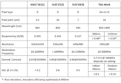
Although the press release does not mention any technical specifications it may be worth referring to an ISSCC paper from 2020 published by a team from Artilux that described a Ge-on-Si technology. The paper is titled "An Up-to-1400nm 500MHz Demodulated Time-of-Flight Image Sensor on a Ge-on-Si Platform" (https://doi.org/10.1109/ISSCC19947.2020.9063107).


Press Release: https://www.artiluxtech.com/resources/news/1014


Go to the original article...

Telluride Neuromorphic Workshop 2022

Image Sensors World        Go to the original article...

The 2022 edition of the Telluride Neuromorphic Workshop series will be held in-person June 26 to July 16 in beautiful Telluride, Colorado. The topics of interest are broadly in "neuromorphic engineering" with neuromorphic vision sensors (including event cameras and other "spiking"-based vision sensors) being key areas of interest.

Neuromorphic engineers design and fabricate artificial neural systems whose organizing principles are based on those of biological nervous systems. Over the past 27 years, the neuromorphic engineering research community focused on the understanding of low-level sensory processing and systems infrastructure; efforts are now expanding to apply this knowledge and infrastructure to addressing higher-level problems in perception, cognition, and learning. In this 3-week intensive workshop and through the Institute for Neuromorphic Engineering (INE), the mission is to promote interaction between senior and junior researchers; to educate new members of the community; to introduce new enabling fields and applications to the community; to promote ongoing collaborative activities emerging from the Workshop, and to promote a self-sustaining research field.

The workshop will be organized in four topic areas

  • Neuromorphic Tactile Exploration (Enhance the tactile exploration capabilities of robots)
  • Lifelong Learning at Scale: From Neuroscience Theory to Robotic Applications (Apply neuro-inspired principles of lifelong learning to autonomous systems.)
  • Cross-modality brain signals: auditory, visual and motor 
  • Neuromorphics Tools, Techniques and Hardware (SpiNNaker 2 and FPAAs)

Researchers from academia, industry and national labs are all encouraged to apply... 

... in particular if they are prepared to work on specific projects, talk about their own work or bring demonstrations to Telluride (e.g. robots, chips, software). 

An application is required to attend, and financial support is available. Application deadline is April 8, 2022.

Call for applications.

Application submission page.

Go to the original article...

Privacy-Aware Cameras for Human Pose Recognition

Image Sensors World        Go to the original article...

Carlos Hinojosa, Juan Carlos Niebles and Henry Arguello published an article titled "Learning Privacy-preserving Optics for Human Pose Estimation" in the 2021 International Conference on Computer Vision which was held virtually in October 2021. This is a collaboration between Universidad Industrial de Santander (Colombia) and Stanford University (USA).


The widespread use of always-connected digital cameras in our everyday life has led to increasing concerns about the users’ privacy and security. How to develop privacy-preserving computer vision systems? In particular, we want to prevent the camera from obtaining detailed visual data that may contain private information. However, we also want the camera to capture useful information to perform computer vision tasks. Inspired by the trend of jointly designing optics and algorithms, we tackle the problem of privacy-preserving human pose estimation by optimizing an optical encoder (hardware-level protection) with a software decoder (convolutional neural network) in an end-to-end framework. We introduce a visual privacy protection layer in our optical encoder that, parametrized appropriately, enables the optimization of the camera lens’s point spread function (PSF). We validate our approach with extensive simulations and a prototype camera. We show that our privacy-preserving deep optics approach successfully degrades or inhibits private attributes while maintaining important features to perform human pose estimation.


They take a "deep-optics" approach --- a learning-based approach where a neural network is used not only to recognize the human pose, but also to train a privacy-preserving point-spread-function (PSF). The neural network is trained to strike a balance between two competing requirements: (a) hiding scene information so that human aces are not recognizable in the RGB images (even after image deblurring), while ensuring that (b) the PSF distortions aren't so strong that the pose-estimation task becomes impossible.


Their results look quite promising, and they even built a proof-of-concept hardware prototype using a wavefront modulator. Notice that the human faces are not recognizable in the RGB images, but the "match-stick" skeletons are still reliably picked out by the algorithm.


More details are in the open access paper and accompanying supplementary document and video available here: https://carloshinojosa.me/project/privacy-hpe/ 

Go to the original article...

Privacy-Aware Cameras for Human Pose Recognition

Image Sensors World        Go to the original article...

Carlos Hinojosa, Juan Carlos Niebles and Henry Arguello published an article titled "Learning Privacy-preserving Optics for Human Pose Estimation" in the 2021 International Conference on Computer Vision which was held virtually in October 2021. This is a collaboration between Universidad Industrial de Santander (Colombia) and Stanford University (USA).


The widespread use of always-connected digital cameras in our everyday life has led to increasing concerns about the users’ privacy and security. How to develop privacy-preserving computer vision systems? In particular, we want to prevent the camera from obtaining detailed visual data that may contain private information. However, we also want the camera to capture useful information to perform computer vision tasks. Inspired by the trend of jointly designing optics and algorithms, we tackle the problem of privacy-preserving human pose estimation by optimizing an optical encoder (hardware-level protection) with a software decoder (convolutional neural network) in an end-to-end framework. We introduce a visual privacy protection layer in our optical encoder that, parametrized appropriately, enables the optimization of the camera lens’s point spread function (PSF). We validate our approach with extensive simulations and a prototype camera. We show that our privacy-preserving deep optics approach successfully degrades or inhibits private attributes while maintaining important features to perform human pose estimation.


They take a "deep-optics" approach --- a learning-based approach where a neural network is used not only to recognize the human pose, but also to train a privacy-preserving point-spread-function (PSF). The neural network is trained to strike a balance between two competing requirements: (a) hiding scene information so that people's faces are not recognizable in the RGB images (even after image deblurring), while ensuring that (b) the PSF distortions aren't so strong that the pose-estimation task becomes impossible.


Their results look quite promising, and they even built a proof-of-concept hardware prototype using a wavefront modulator. Notice that the human faces are not recognizable in the RGB images, but the "match-stick" skeletons are still reliably picked out by the algorithm.


More details are in the open access paper and accompanying supplementary document and video available here: https://carloshinojosa.me/project/privacy-hpe/ 

Go to the original article...

New Author Introduction – Atul Ingle

Image Sensors World        Go to the original article...

Atul Ingle has kindly agreed to help me publishing the posts and also give his unique view on image sensor from computer vision developer point of view.

Atul Ingle is an Assistant Professor in the Department of Computer Science at Portland State University. His research interests are in the fields of computational imaging, computer vision and signal processing. His current research involves co-design of imaging hardware and algorithms for single-photon image sensors. More broadly, he is interested in both passive and active 3D imaging applications that are severely resource-constrained in terms of power, bandwidth, and compute. Atul holds a PhD in Electrical and Computer Engineering from University of Wisconsin-Madison.

Go to the original article...

New Author Introduction – Saleh Masoodian

Image Sensors World        Go to the original article...

I'd guess many of you know Saleh Masoodian, CEO of Gigajot. I'm happy to announce that Saleh has kindly agreed to join the authors of the blog.

With Mark and Saleh, the new blog would offer quite diverse views on the industry.

Go to the original article...

Fujifilm INSTAX mini EVO review

Cameralabs        Go to the original article...

The INSTAX mini EVO is a digital instant camera with a screen and a built-in printer to make physical copies. It can also be used as a wireless printer for your phone. But does it lack the vintage charm we know and love from analogue INSTAX cameras? Find out in my review!…

Go to the original article...

Optimizing Machine Vision Lenses For Different Wavelengths

Image Sensors World        Go to the original article...

 Quality Magazine publishes an article covering consideration when Optimizing Machine Vision Lenses For Different Wavelengths.

"Lenses play a crucial role in the quality of the images produced by a machine vision system since they determine the sharpness of the image on the camera sensor. Lenses can influence image quality in a variety of ways:
  • Reduced light transmission due to lens surface reflections
  • Spherical, chromatic and defect aberrations preventing all rays of light from a single point on the object being focused to a single point on the image
  • Reduced light intensity towards the edge of the image
  • Spatial distortion of the image

By choosing the appropriate lens construction, all of these effects can be minimized. This article highlights some of the considerations when selecting a lens for your particular needs."


Go to the original article...

New Author Introduction – Mark Sapp

Image Sensors World        Go to the original article...

Dear Image Sensors World Blog readers,

Let me introduce Mark Sapp who kindly offered a help with posting the image sensor news in the blog. Mark is an electrical engineer working in the industry for 15 years and an enthusiast for cutting edge imaging technology, located in Austin, Texas. Mark, welcome to the community!

If somebody wants to post more news in the blog, please let me know and I'd gladly add you to the list of authors. I hope that this enriches the blog content and add more diverse views from the different branches of the industry.

Go to the original article...

Suspension of the Blog

Image Sensors World        Go to the original article...

Due to a large workload, I'm unable to continue publishing the blog. So, the blog is suspended for the time being.

Go to the original article...

303-Megaframes-per-Second Image Sensor

Image Sensors World        Go to the original article...

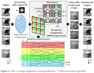
MDPI starts publishing a Special Issue on Recent Advances in CMOS Image Sensor with a paper "A Dual-Mode 303-Megaframes-per-Second Charge-Domain Time-Compressive Computational CMOS Image Sensor" by Keiichiro Kagawa, Masaya Horio, Anh Ngoc Pham, Thoriq Ibrahim, Shin-ichiro Okihara, Tatsuki Furuhashi, Taishi Takasawa, Keita Yasutomi, Shoji Kawahito, and Hajime Nagahara from Shizuoka University and Osaka University.

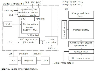
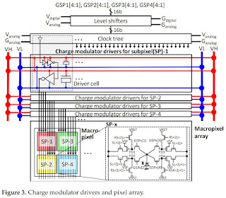
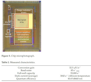
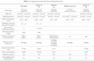
"An ultra-high-speed computational CMOS image sensor with a burst frame rate of 303 megaframes per second, which is the fastest among the solid-state image sensors, to our knowledge, is demonstrated. This image sensor is compatible with ordinary single-aperture lenses and can operate in dual modes, such as single-event filming mode or multi-exposure imaging mode, by reconfiguring the number of exposure cycles. To realize this frame rate, the charge modulator drivers were adequately designed to suppress the peak driving current taking advantage of the operational constraint of the multi-tap charge modulator. The pixel array is composed of macropixels with 2 × 2 4-tap subpixels. Because temporal compressive sensing is performed in the charge domain without any analog circuit, ultrafast frame rates, small pixel size, low noise, and low power consumption are achieved. In the experiments, single-event imaging of plasma emission in laser processing and multi-exposure transient imaging of light reflections to extend the depth range and to decompose multiple reflections for time-of-flight (TOF) depth imaging with a compression ratio of 8× were demonstrated. Time-resolved images similar to those obtained by the direct-type TOF were reproduced in a single shot, while the charge modulator for the indirect TOF was utilized."

Go to the original article...

303-Megaframes-per-Second Image Sensor

Image Sensors World        Go to the original article...

MDPI starts publishing a Special Issue on Recent Advances in CMOS Image Sensor with a paper "A Dual-Mode 303-Megaframes-per-Second Charge-Domain Time-Compressive Computational CMOS Image Sensor" by Keiichiro Kagawa, Masaya Horio, Anh Ngoc Pham, Thoriq Ibrahim, Shin-ichiro Okihara, Tatsuki Furuhashi, Taishi Takasawa, Keita Yasutomi, Shoji Kawahito, and Hajime Nagahara from Shizuoka University and Osaka University.

"An ultra-high-speed computational CMOS image sensor with a burst frame rate of 303 megaframes per second, which is the fastest among the solid-state image sensors, to our knowledge, is demonstrated. This image sensor is compatible with ordinary single-aperture lenses and can operate in dual modes, such as single-event filming mode or multi-exposure imaging mode, by reconfiguring the number of exposure cycles. To realize this frame rate, the charge modulator drivers were adequately designed to suppress the peak driving current taking advantage of the operational constraint of the multi-tap charge modulator. The pixel array is composed of macropixels with 2 × 2 4-tap subpixels. Because temporal compressive sensing is performed in the charge domain without any analog circuit, ultrafast frame rates, small pixel size, low noise, and low power consumption are achieved. In the experiments, single-event imaging of plasma emission in laser processing and multi-exposure transient imaging of light reflections to extend the depth range and to decompose multiple reflections for time-of-flight (TOF) depth imaging with a compression ratio of 8× were demonstrated. Time-resolved images similar to those obtained by the direct-type TOF were reproduced in a single shot, while the charge modulator for the indirect TOF was utilized."

Go to the original article...

Pixel Crosstalk in 2-Layer Sensors

Image Sensors World        Go to the original article...

MPDP publishes a paper "Parasitic Coupling in 3D Sequential Integration: The Example of a Two-Layer 3D Pixel" by Petros Sideris, Arnaud Peizerat, Perrine Batude, Gilles Sicard, and Christoforos Theodorou from University Grenoble Alpes which is the extended version of the paper presented at 10th International Conference on Modern Circuits and Systems Technologies (MOCAST), Thessaloniki, Greece, 5–7 July 2021.

"In this paper, we present a thorough analysis of parasitic coupling effects between different electrodes for a 3D Sequential Integration circuit example comprising stacked devices. More specifically, this study is performed for a Back-Side Illuminated, 4T–APS, 3D Sequential Integration pixel with both its photodiode and Transfer Gate at the bottom tier and the other parts of the circuit on the top tier. The effects of voltage bias and 3D inter-tier contacts are studied by using TCAD simulations. Coupling-induced electrical parameter variations are compared against variations due to temperature change, revealing that these two effects can cause similar levels of readout error for the top-tier readout circuit. On the bright side, we also demonstrate that in the case of a rolling shutter pixel readout, the coupling effect becomes nearly negligible. Therefore, we estimate that the presence of an inter-tier ground plane, normally used for electrical isolation, is not strictly mandatory for Monolithic 3D pixels."

Go to the original article...

Sony UV Image Sensor Video

Image Sensors World        Go to the original article...

Sony publishes a promotional video about its IMX487 UV sensor:

Go to the original article...

Article about Peter Noble and his Early Image Sensors

Image Sensors World        Go to the original article...