Image Sensors World Go to the original article...
BeyonSense-Stratio-LinkSquare demos its SWIR Ge-based sensor capabilities:
Visual Industry Guide
Image Sensors World Go to the original article...
BeyonSense-Stratio-LinkSquare demos its SWIR Ge-based sensor capabilities:
Image Sensors World Go to the original article...
Yole Developpement report "Thermal Imagers and Detectors 2020" updates:
"The current surge of EST [elevated body or surface temperature] applications has transformed the thermal imager manufacturer landscape, at least for thermography. In 2019, US and EU players (FLIR, Lynred, SEEK) were leading this market. Enter COVID-19, and Chinese players (Guide IR, Hikvision, Iray) have turned the tables, surpassing the market leaders, at least in shipments. They rapidly addressed the great domestic demand for thermal imaging systems. Having acquired in the past few years technical competences in thermal imager manufacturing, these Chinese players ramped up their domestic production during the last 2 years, and the current situation has fueled their path to becoming stars. As the epidemic spread across geographies to the west, the rest of the companies reaped the benefits from this hype. But western countries were slower in adopting thermal cameras en masse, due to privacy concerns.
In general, thermal imager production lines are not like other integrated circuit (IC) production lines that work at more than 90% of production capacity. Therefore, for some companies there was not a particular need for investment, besides some increase in consumables and possibly workforce. But for some Chinese companies, it is highly possible that the government has supported their production ramp ups. Moreover, this situation could push Chinese companies to chase investments for future growth, which could rapidly develop the market in the future.
But what could happen next year? Chinese manufacturers have enormous production capacity which risks being left unused. We could be spectators to huge changes in strategy where they could:
At this point, many uncertainties exist. One thing is sure: exciting times lie ahead for the thermal imaging industry."


Image Sensors World Go to the original article...
Arxiv.org paper "HDR Imaging with Quanta Image Sensors: Theoretical Limits and Optimal Reconstruction" by Abhiram Gnanasambandam and Stanley H. Chan from Purdue University shows DR advantage of QIS over CIS:
"High dynamic range (HDR) imaging is one of the biggest achievements in modern photography. Traditional solutions to HDR imaging are designed for and applied to CMOS image sensors (CIS). However, the mainstream one-micron CIS cameras today generally have a high read noise and low frame-rate. These, in turn, limit the acquisition speed and quality, making the cameras slow in the HDR mode. In this paper, we propose a new computational photography technique for HDR imaging. Recognizing the limitations of CIS, we use the Quanta Image Sensor (QIS) to trade the spatial-temporal resolution with bit-depth. QIS is a single-photon image sensor that has comparable pixel pitch to CIS but substantially lower dark current and read noise. We provide a complete theoretical characterization of the sensor in the context of HDR imaging, by proving the fundamental limits in the dynamic range that QIS can offer and the trade-offs with noise and speed. In addition, we derive an optimal reconstruction algorithm for single-bit and multi-bit QIS. Our algorithm is theoretically optimal for all linear reconstruction schemes based on exposure bracketing. Experimental results confirm the validity of the theory and algorithm, based on synthetic and real QIS data."


Image Sensors World Go to the original article...
Brookman compares continuous and pulsed iToF approaches with respect to the tolerance to ambient light:
Image Sensors World Go to the original article...
BusinessWire: SmartSens Founder and CEO Richard Xu received a 2020 Innovator of the Year Award at ASPENCORE Global High-Tech Executive Forum.
In an interview with ASPENCORE China analyst, Xu comments on the future of SmartSens:
“As a CMOS image sensor chip design company driven by innovation, SmartSens has selected the technically demanding security product industry as a market entry point. We’ve able to take advantage of the country’s rapid advancements and explosive growth in smart cities and intelligent transportation to become a leader in this field.
In particular, our ultra-starlight-level full-color night vision imaging technology, Stack BSI Global Shutter technology, single-frame HDR technology, and Near-Infrared Enhancement technology among others that have garnered recognitions by leading customers in the security industry.”
Regarding the future of semiconductor industry in China, Xu says:
“Currently, the country can only provide 15% of the overall chip supply, while the demand is over 50%. In addition, there is a demand for high-end chip customization. This presents an opportunity for the domestic semiconductor industry to tap into this rapid development.
From a more passive point of view, it means that domestic companies must examine their own potential. Technological innovation is the key. With a global strategy and strong national sentiment, as well as respect of intellectual property and common-ground value, the market will prove that a win-win situation is attainable.”

Image Sensors World Go to the original article...
BusinessWire: ON Semiconductor introduces a single point dToF LiDAR solution based on the company's Silicon Photomultiplier (SiPM). The SiPM dToF LiDAR Platform can detect objects at distances between 10 cm and 23 m.
The SiPM dToF LiDAR Platform provides a complete solution for low cost, single point LiDAR that OEMs can adapt and take into production to create industrial range finding applications. It includes the NIR laser diode, SiPM sensor and optics, as well as the digital processing necessary to convert the detected signals into elapsed time, and elapsed time into distance.


BusinessWire: Luminar makes a number of public announcements toward closing its reverse merging IPO deal:
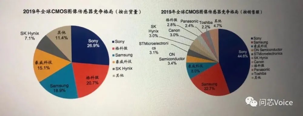
Image Sensors World Go to the original article...
Yole Developpement report "The CIS industry overheated in 2019 reaching $19.3B. Are we heading to a soft landing in 2020-2021?" says:
"At the top of the market, player trajectories are a consequence of the smartphone market situation. Sony and Samsung are first and second and Omnivision third. ST Microelectronics is in fourth position, making a comeback thanks to its near infrared (NIR) sensing imagers for Apple handsets and tablets. Sony and Samsung have subsequently updated their product portfolio in line with the 3D sensing trend. Indirect Timeof-Flight (iToF) and direct Time-of-Flight (dToF) arrays are the immediate response, showing the great technical innovation driving those top players.
On the other side of the market, emerging players to watch are coming from China. Omnivision has been acquired by Will Semiconductor, the Shanghai-based company. Two other Chinese players, Galaxycore
and Smartsens, are also experiencing thriving growth. They have mostly benefited from their domestic market ecosystem in mobile and security cameras. Their growth is currently fueled by massive capital injections at time of greater US sanctions limiting their access to technology. CIS might be among the first semiconductor product categories in which China could become technologically independent since the required wafer foundries are widely available in mainland China.
The next era will involve robotics, Augmented Reality (AR) and smart Internet of Things (IoT). All of these are markets in which Chinese companies are well positioned. The ranking of CIS players will eventually change along these new lines."


Image Sensors World Go to the original article...
EDN publishes camera tutorial by Richard Crisp, Etron VP of New Product Development. Its third part about rolling and global shutter has a nice visualization of the dark current statistics:

Image Sensors World Go to the original article...
Infineon's quarterly Investor Presentation shows the company's forecast of ToF sensor market:


Image Sensors World Go to the original article...
Sohu (via IFNews), Zaotech: Gigadevice Director of ToF Marketing of the Sensor Division Haolei Liu presents the company plans to develop ToF sensors and optical fingerprint sensors for smartphones:
"GigaDevice’s innovative ToF solution adopts a special process, has a higher QE, can effectively reduce power consumption and system cost, and can support both the 1350nm-1550nm long wavelength band and the 940nm wavelength band. Outdoors have excellent performance, which meets the needs of the future screen direction.
Liu Haolei also pointed out: “In our opinion, iToF and dToF will be parallel for a period of time. Although the resolution is a shortcoming of dToF, in the long run, we believe that dToF has a lot of room for growth because of the dToF solution. Not long after its launch, the industrial chain is not mature, which also means that it has a lot of room for improvement.
We believe that the potential of ToF needs to be promoted by industry chain ecological partners. It is certain that this technology will have higher and higher requirements for hardware . For example, resolution. In the dToF solution, if the resolution can be significantly improved, the application of products will become more and more extensive.”
The new GigaDevice's ToF sensor is said to have QVGA resolution, QE of 65% at 940nm or 50% at 1350nm, "which is nearly double that of the ToF chip based on silicon technology."

MEMSensor: The company also develops a new α-Si process-based under OLED-screen optical fingerprint sensor named GSL7253. It's said to have a sensitive area of 20x30mm2, a QE of 80%, and is only 0.3mm thin:


Image Sensors World Go to the original article...
A number of Ebay sellers offer "research" 8-inch image sensor wafers for $25 a piece. Possibly, they could serve as a nice souvenir:


Image Sensors World Go to the original article...
FinanceSecond, NetEase: GalaxyCore listing at Science and Technology Innovation Board of the Shanghai Stock Exchange has been approved by authorities. The IPO includes 15% share of the company at the price of 7,428,830,300 RMB (about $1.124B). This values the company at $7.5B.
The money will be invested into CIS R&D and 12-inch wafer BSI processing facility that Galaxycore built in Lingang New Area of China (Shanghai) Free Trade Pilot Zone.
"Through the construction of some 12-inch BSI wafer back-end production lines, 12-inch wafer manufacturing pilot lines, some OCF manufacturing and back grinding and cutting production lines, the company has realized the transition from the Fabless model to the Fab-Lite model."


Image Sensors World Go to the original article...
BusinessWire: As a public company, Velodyne reports its quarterly results, giving a good food for thought about LiDAR market as a whole:
Image Sensors World Go to the original article...
BusinessWire: Ambarella introduces the CV28M camera SoC, the latest in the CVflow family, combining image processing, high-resolution video encoding, and CVflow computer vision processing in a single, low-power design. The CV28M’s efficient AI architecture provides the flexibility to enable a new class of smart edge devices for applications including smart home security, retail monitoring, consumer robotics, and occupancy monitoring.
“All around us, devices are becoming smarter, and with our newest CV28M SoC, our customers can develop a new generation of intelligent sensing cameras for a variety of new applications,” said Chris Day, VP of marketing and business development at Ambarella. “In privacy-sensitive applications—such as monitoring retail stores, workplaces, rental properties, or the elderly at home—edge-based AI processing can support intelligent monitoring and fast decision-making without the requirement to record or stream video to the cloud.”

ON Semi publishes a promotional video about its SiPM use in dToF laser rangefinders:


Image Sensors World Go to the original article...
Soitec says that its "Imager-SOI [wafer] product line is designed specifically for fabricating front-side imagers for near-infrared (NIR) applications including advanced 3D image sensors."


Image Sensors World Go to the original article...
Soitec says that its "Imager-SOI [wafer] product line is designed specifically for fabricating front-side imagers for near-infrared (NIR) applications including advanced 3D image sensors."
Image Sensors World Go to the original article...
Waterloo Institute for Nanotechnology is going to design sub-micron pixels for X-Ray ptychography. In regular X-ray sensors, the pixel pitch is 100-200um or more.
Image Sensors World Go to the original article...
IC-Insights forecasts a slight growth of image sensor market this year, followed by a 12% growth in 2021:

Image Sensors World Go to the original article...
Samsung unveils its first iTOF product - ISOCELL Vizion 33D:
"Featuring 4-tap pixels, the Samsung ISOCELL Vizion 33D delivers precise and swift depth sensing capabilities for next-level 3D applications.
Enabling pro-grade shots with bokeh effects or accurate 3D object images, the ToF (Time-of-Flight) sensor is optimized to provide best-in-class photography and AR/VR experiences.
To enable precise depth measurement of fast-moving objects, the ISOCELL Vizion 33D features a 4-tap demodulation system and supports frame rate of up to 120fps. Each pixel in the sensor can receive four phase signals simultaneously (0°, 90°, 180°, and 270°), which means it can generate a depth image with just a single frame. The ISOCELL Vizion 33D can capture moving objects with significant reduction of motion artifacts.
In both indoor and outdoor conditions, the sensor can detect the depth of an object within up to 5m with high accuracy. ISOCELL’s pixel technology, coupled with high resolution, enables the sensor to accurately separate objects from the background with 3D bokeh effect.
Deep Trench Isolation technology (DTI) maximizes isolation between pixels to reduce crosstalk, while Backside Scattering Technology (BST) enhances the sensor’s quantum efficiency. With high-precision depth images, the ISOCELL Vizion 33D delivers next-level 3D applications, such as facial authentication for payment services.
With a total power consumption of under 400mW for both IR illuminator and the ToF sensor, the 33D makes it possible for users to enjoy powerful 3D features, such as AR games and video bokeh, throughout the day."



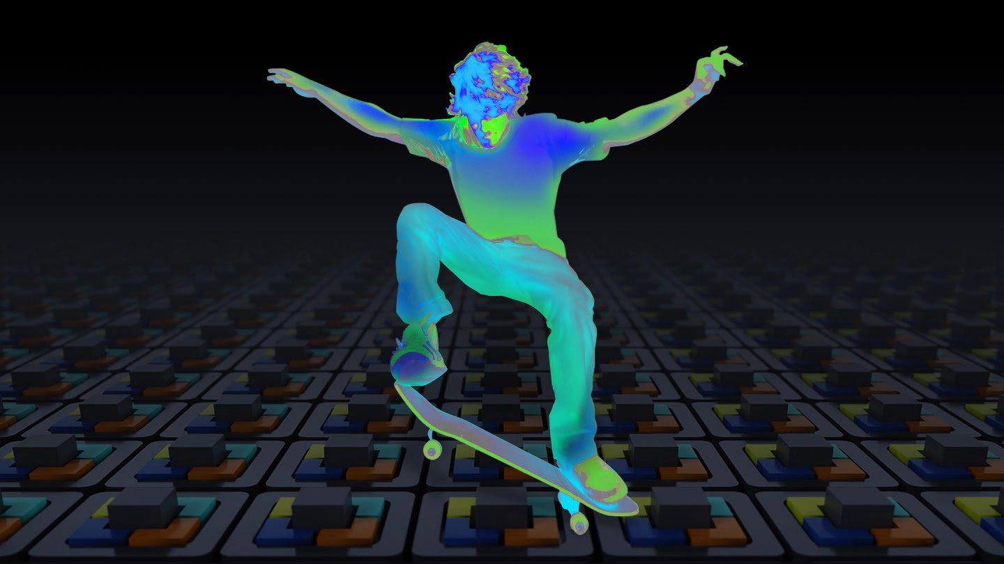
Image Sensors World Go to the original article...
Zeiss Visioner 1 digital microscope uses SD Optics' Micro-mirror Array Lens System (MALS) technology to achieve digitally-extended depth of focus up to 69mm:
"ZEISS Visioner 1 revolutionizes the world of optical inspection and documentation. Driven by the unique Micro-mirror Array Lens System (MALSTM technology), enables for the first time, real-time all-in-focus imaging – first time, every time.
Using a micro-mirror array lens system (MALS™) enables us to generate “virtual” lenses with distinctly different curvatures, thus different focus planes. This is achieved by changing the orientation of each individual micro-mirror in an orchestrated way.
Re-shaping the curvature of this “virtual” lens at speed enables ultra-fast focusing and real-time all-in focus imaging and documentation."

Image Sensors World Go to the original article...
IEDM publishes its 2020 program with many image sensor-related papers:Image Sensors World Go to the original article...
PRNewswire: 3 year-old FMCW LiDAR startup Aeva announces a reverse merging with InterPrivate Acquisition Corp. to be listed on NYSE at $2.1B valuation. This transaction is to provide up to $363M in gross proceeds, comprised of InterPrivate's $243M held in trust and a $120M fully committed common stock PIPE at $10.00 per share, including investments from Adage Capital and Porsche SE.
The combined company expected to have an estimated post-transaction equity value of approximately $2.1B and is expected to be listed on the NYSE under the ticker symbol AEVA following anticipated transaction close in Q1 2021.


Image Sensors World Go to the original article...
BusinessKorea tells: "Sony’s image sensor sales are predicted to fall from 240 billion yen in the second quarter of this year to 130 billion yen in the second quarter of next year.
This is leading to an opportunity for Samsung. The latecomer in the industry has focused on Xiaomi, Vivo and others rather than Huawei.
Samsung is aiming to rise to the top in the global image sensor market by 2030. Last year, Samsung’ share in the market was 18.1 percent and Sony’s was 53.5 percent."
Image Sensors World Go to the original article...
Livox announces two new products, Mid-70 and AVIA:

Voyant Photonics President Peter Stern talks about Apple LiDAR:
"The iPhone time-of-flight LiDAR, probably built with the same amazing SPAD array used in the iPad, coupled with a VCSEL array for illumination, is an engineering marvel. It’s absolute magic.
After working on LiDAR three decades ago that could detect telephone lines kilometers away from a fast-moving, low-flying helicopter, I have been waiting for this kind of LiDAR magic for a long time.
At Voyant, we have a different approach. No VCSELs, no SPADs. Adapting microscopic optical components from datacom chips to active sensing, we have created a coherent pixel array for LiDAR, similar to the ubiquitous CMOS image sensors found everywhere. Each pixel both transmits and receives light at 1550 nm wavelengths.


Cameralabs Go to the original article...
The Moon is one of my favourite subjects to photograph and in this tutorial I'll show you how to take great photos of it including exposure, phases, Earthshine and how to plan a Moon-rise with a landscape in the foreground!…
The post Moon Photography Tutorial appeared first on Cameralabs.
Image Sensors World Go to the original article...
APL Photonics paper "An optical chip for self-testing quantum random number generation" by Nicolò Leone, Davide Rusca, Stefano Azzini, Giorgio Fontana, Fabio Acerbi, Alberto Gola, Alessandro Tontini, Nicola Massari, Hugo Zbinden, and Lorenzo Pavesi from University of Trento, FBK, and University of Geneva describes how photon shot noise-based RNG is built:
"We present an implementation of a semi-device-independent protocol of the generation of quantum random numbers in a fully integrated silicon chip. The system is based on a prepare-and-measure scheme, where we integrate a partially trusted source of photons and an untrusted single photon detector. The source is a silicon photomultiplier, which emits photons during the avalanche impact ionization process, while the detector is a single photon avalanche diode. The proposed protocol requires only a few and reasonable assumptions on the generated states. It is sufficient to measure the statistics of generation and detection in order to evaluate the min-entropy of the output sequence, conditioned on all possible classical side information. We demonstrate that this protocol, previously realized with a bulky laboratory setup, is totally applicable to a compact and fully integrated chip with an estimated throughput of 6 kHz of the certified quantum random bit rate."

Image Sensors World Go to the original article...
MDPI paper "How Good Are RGB Cameras Retrieving Colors of Natural Scenes and Paintings?—A Study Based on Hyperspectral Imaging" by João M. M. Linhares, José A. R. Monteiro, Ana Bailão, Liliana Cardeira, Taisei Kondo, Shigeki Nakauchi, Marcello Picollo, Costanza Cucci, Andrea Casini, Lorenzo Stefani, and Sérgio Miguel Cardoso Nascimento from University of Minho, University of Lisbon, Portuguese Catholic University (Portugal), Toyohashi University of Technology (Japan), and Istituto di Fisica Applicata “Nello Carrara” del Consiglio Nazionale delle Ricerche (Italy), describes an interesting experiment:
"RGB digital cameras (RGB) compress the spectral information into a trichromatic system capable of approximately representing the actual colors of objects. Although RGB digital cameras follow the same compression philosophy as the human eye (OBS), the spectral sensitivity is different. To what extent they provide the same chromatic experiences is still an open question, especially with complex images. We addressed this question by comparing the actual colors derived from spectral imaging with those obtained with RGB cameras. The data from hyperspectral imaging of 50 natural scenes and 89 paintings was used to estimate the chromatic differences between OBS and RGB. The corresponding color errors were estimated and analyzed in the color spaces CIELAB (using the color difference formulas ΔE*ab and CIEDE2000), Jzazbz, and iCAM06. In CIELAB the most frequent error (using ΔE*ab) found was 5 for both paintings and natural scenes, a similarity that held for the other spaces tested. In addition, the distribution of errors across the color space shows that the errors are small in the achromatic region and increase with saturation. Overall, the results indicate that the chromatic errors estimated are close to the acceptance error and therefore RGB digital cameras are able to produce quite realistic colors of complex scenarios."


