Image Sensors World Go to the original article...
IEEE Buenaventura Section publishes a presentation "Evolution of Scientific Image Sensor ICs - Past, Present, and Future" by Atul Joshi , CEO and chief innovation officer of SAAZ Micro Inc.
Visual Industry Guide
Image Sensors World Go to the original article...
IEEE Buenaventura Section publishes a presentation "Evolution of Scientific Image Sensor ICs - Past, Present, and Future" by Atul Joshi , CEO and chief innovation officer of SAAZ Micro Inc.
Image Sensors World Go to the original article...
Terranet CTO Nihat Kücük presents BlincVision combining structured light 3D imaging with event-driven sensor: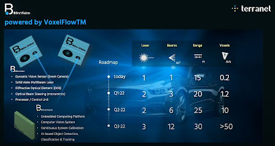
Image Sensors World Go to the original article...
ETH Zurich publishes "ESL: Event-based Structured Light" project page by M. Muglikar, G. Gallego, and D. Scaramuzza.Image Sensors World Go to the original article...
Imec has updated its page on SWIR imagers, including a new Vimeo video:
The Pixel Technology Explore activity is looking at two methods for cost-effective uncooled IR detection:
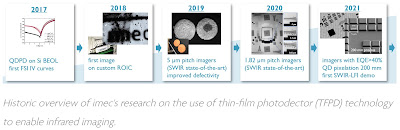
Image Sensors World Go to the original article...
Luminar co-founder and CTO Jason Eichenholz discusses the company’s acquisition of its exclusive InGaAs sensor provider and advantages of the SWIR LiDAR photon budget:Image Sensors World Go to the original article...
BusinessWire: SiLC launches the new Eyeonic LiDAR providing accurate instantaneous depth, velocity, and dual-polarization intensity information while enabling immunity to multi-user and environmental interference. No performance data has been released.
“Eyeonic will be transformational to many industries across the globe by enabling the anticipated mass migration to coherent imaging,” explained Mehdi Asghari, founder and CEO, SiLC. “Our unique technology and innovative manufacturing process puts SiLC in the optimal position to provide the key building blocks needed for this next wave of significant innovation – at a competitive price.”


Image Sensors World Go to the original article...
MIPI publishes a video introduction into different D-PHY standards:
Image Sensors World Go to the original article...
Nikkei-Asia: Canon plans to start mass-production of the 3.2MP SPAD sensor for security cameras in 2022. The sensor is said to provide a color night vision, as well as ToF feature:


Image Sensors World Go to the original article...
Lucid Vision presents its SWIR camera based on Sony SenSWIR InGaAs stacked sensor:
Image Sensors World Go to the original article...
Aiji Micro App: According to Qunzhi Consulting’s (English name Sigmaintell) market report, global smartphone CIS shipments in Q3 2021 were approximately 1.21B, a YoY decline of approximately 24.0%. Qunzhi Consulting estimates that global smartphone image sensor shipments in 2021 will be approximately 5.05B, a YoY decrease of 10.3%:
Image Sensors World Go to the original article...
Tecno Mobile publishes a webinar "Mobile Camera Trends 2022: Innovation Talk:"
Image Sensors World Go to the original article...
Sony publishes a white paper promoting its InGaAs SWIR sensors:


Image Sensors World Go to the original article...
MIPI Alliance has recently released the Camera Service Extensions (MIPI CSESM) v1.0 specification, which enhances the MIPI Camera Serial Interface 2 (MIPI CSI-2) image sensor interface with end-to-end functional safety and other features for automotive applications:

Image Sensors World Go to the original article...
EETimes: Pixart launches Single-Axis Distance Sensor (SAS) product line based on the optical-geometric technology. There are two sensors in the new product line: PAC7088J1 is a middle-range version and PAC7088J2 is s short range one.


Image Sensors World Go to the original article...
Hamamatsu publishes a new flyer for its Orca-Quest qCMOS camera with example applications for its photon resolving capability:


Image Sensors World Go to the original article...
PRNewswire: Xailient announces face recognition AI for Sony's intelligent vision sensor IMX500 with 97.8% accuracy up to 3 meters distance. On the IMX500, Xailient claims to provide the world's most power-efficient Face Recognition AI.

Image Sensors World Go to the original article...
ISSCC publishes its 2022 Agenda. There are 13 image sensor-related papers:
Image Sensors World Go to the original article...
Rice University publishes an OSA Optica paper "EDoF-ToF: extended depth of field time-of-flight imaging" by Jasper Tan, Vivek Boominathan, Richard Baraniuk, and Ashok Veeraraghavan.
Image Sensors World Go to the original article...
During the recent Qualcomm's mobile processor announcements, there was a part on establishing a joint lab with Sony in San Diego working on image sensor and processor co-optimization:
Image Sensors World Go to the original article...
BAE (Fairchild Imaging) presents 12MP 240fps APS-C sensor LTN4625A with global and rolling shutter modes:
Image Sensors World Go to the original article...
GlobeNewswire: Advantest has begun shipping the fourth generation of its high-speed image-processing engine that applies heterogeneous computing technology to detect defects in the data output from CMOS image sensors. When integrated on the proven T2000 ISS platform, the new T2000 IP Engine 4 (Image Processing Engine 4) system provides the means of evaluating the latest high-resolution, high-speed CIS devices used in advanced smart phone cameras.


Image Sensors World Go to the original article...
Qualcomm announces its next generation mobile processor Snapdragon 8 Gen 1:


Image Sensors World Go to the original article...
iNews, Lieyunwang, iFeng: Guangzhou Tyrafos (Chinese name Guangzhou Yinxin Semiconductor Technology Co., Ltd.) announces the A+ round of financing led by Yunqi Capital. By the end of this round of financing, Yinxin Semiconductor is expected to receive hundreds of millions of yuan in the near future.
Tyrafos also announces announced the release of "the world's first non-single photon dToF" (possibly, they mean dToF that is not based on SPADs) and ELISA molecular biological detection solution basedon image sensors.
"The world's first non-single-photon dToF released by Yinxin Semiconductor is the world's first technical solution to achieve direct ToF using CMOS process. Not only the accuracy and resolution are several times higher than the existing SPAD (Single Photon Avalanche Diode) solution. In addition, the overall power consumption of the laser light source at the transmitting end and the sensor at the receiving end has been reduced by 90%, catching up with the core technology of foreign manufacturers such as Apple and STMicroelectronics in this field, and the underlying architecture and circuit IP are independently developed by Yinxin Semiconductor, it solves the technical problem of the neck stuck in the field of 3D perception, and is a milestone breakthrough in the field of 3D perception."


"In the field of fingerprints under the optical screen, Yinxin Semiconductor adopts the innovative design of pixel architecture level to break through the area and cost limits. The chip area is 30%~50% smaller than that of competing products, and the module volume is more than half smaller than that of competing products. It has an ultra-high cost performance. Competitive advantage, in 2019, through cooperation with customers, it became the first optical under-screen fingerprint recognition solution certified by South Korea's Samsung mobile phone. At present, Yinxin Semiconductor has reached an agreement with 4-5 global leading fingerprint solution providers to purchase under-screen fingerprint chips. Intentional orders are expected to contribute hundreds of millions of yuan in revenue."


"The world's first digital ELISA molecular biological detection solution released by Yinxin Semiconductor is the world's first digital solution that directly performs molecular biological detection on the surface of an image sensor. Enzyme Linked Immunosorbent Assay (Enzyme Linked Immunosorbent Assay, abbreviated ELISA or ELASA) refers to a qualitative and quantitative detection method that combines soluble antigens or antibodies on solid-phase carriers such as polystyrene, and uses antigen-antibody specific binding for immunoreaction. . Taking advantage of the company's advantages in high-speed and high-sensitivity image sensors, Yinxin Semiconductor has created a complete set of micro-molecular biological detection equipment based on ELISA standards, achieving a zero breakthrough in this field, and surpassing the United States in detection accuracy and speed. NASDAQ listed company Quanterix (the core technology comes from the Harvard University technical team, the technology founder David Walt is an academician of the American Academy of Engineering and the Medical School, and is also the scientific founder of Illumina) SiMoA (Single-molecule Array) system, and Yinxin Semiconductor In terms of equipment cost and consumables cost, the digital ELISA technology of the company has a significant improvement over Quanterix's SiMoA system technology. The sensitivity of the digital ELISA technology is more than 1000 times higher than that of the traditional ELISA. Its appearance brings protein detection technology directly into the era of single-molecule and digital detection, becoming the true king in the field of fg-level ultra-low abundance protein detection. The optimization of detection accuracy, speed and cost is more conducive to application promotion. In the future, it will have great application potential in the fields of coronavirus detection, influenza virus detection, and early cancer screening."

Tyrafos has been established in May 2019 and its core team coming from TI, Omnivision, Samsung, Himax, TSMC, Mediatek, ASE, Foxconn, and Chi Mei. The company has >90 full-time R&D and operations employees. The core members of the team have 15-20 years experience in the semiconductor industry. The company names Sony and Samsung as its strategic partners, and TSMC, Samsung, and Tower as its foundries.

Image Sensors World Go to the original article...
Lucid Vision Labs publish an explanatory video about Sony IMX490 5.4MP automotive sensor:
Lucid Vision Labs also publishes a measured EMVA1288 performance of the sensor:

Image Sensors World Go to the original article...
Nature paper "Silicon: quantum dot photovoltage triodes" by Wen Zhou, Li Zheng, Zhijun Ning, Xinhong Cheng, Fang Wang, Kaimin Xu, Rui Xu, Zhongyu Liu, Man Luo, Weida Hu, Huijun Guo, Wenjia Zhou & Yuehui Yu from Chinese Academy of Sciences and ShanghaiTech University presents a concept of 1550nm photodetector with internal gain:

