Image Sensors World Go to the original article...
First part of RSIP webinar series on automotive AI talks about ways to sense depth in ADAS and autonomous driving applications:ToF News: Broadcom, Renesas, Opnous
July 21, 2019 By Leave a Comment
Image Sensors World Go to the original article...
ToF market becomes rather crowded. Many companies enter it anticipating a fast growth.Broadcom AFBR-S50MV85G is APD pixel-based distance and motion measurement ToF sensor. It supports up to 3000 frames per second with up to 16 illuminated pixels. The sensor is aimed to industrial applications and gesture sensing and is said to have best-in-class ambient light suppression of up to 200k Lux. So, the use in outside environments should not be a problem.
Features:
- Integrated 850 nm laser light source
- Between 7-16 illuminated pixels
- FoV of up to 12.4°x 6.2°
- Very fast measurement rates of up to 3 kHz
- Variable distance range up to 10m
- Operation up to 200k Lux ambient light
- Works well on all surface conditions
- Laser Class 1 eye safe ready
- Accuracy better than 1%
- Drop-in compatible within the AFBR-S50 sensor platform


Renesas ISL29501 (Intersil) ToF processor external emitter and detector. The sensor operates on i-ToF in-phase/out-phase priciple:


Shanghai, China-based Opnous offers a number of ToF sensors with different resolutions:


Recent Image Sensor Videos: Omnivision, Prophesee, Intel
July 20, 2019 By Leave a Comment
Image Sensors World Go to the original article...
Omnivision publishes its CEO Boyd Fowler explanation of HALE technology:Prophesee CMO Guillaume Butin presents another use case of its event-driven sensors, vibration monitoring:
Other Prophesee videos explain differences between event-driven and frame-based sensors:
Intel explains how its coded light 3D camera works:
LiDAR News: Voyant Photonics, Aeye
July 19, 2019 By Leave a Comment
Image Sensors World Go to the original article...
Techcrunch: NYC-based LiDAR startup Voyant Photonics raises $4.3M investment from Contour Venture Partners, LDV Capital and DARPA. The founding team of the startup came from Lipson Nanophotonics Group at Columbia University."In the past, attempts in chip-based photonics to send out a coherent laser-like beam from a surface of lightguides (elements used to steer light around or emit it) have been limited by a low field of view and power because the light tends to interfere with itself at close quarters.
Voyant’s version of these “optical phased arrays” sidesteps that problem by carefully altering the phase of the light traveling through the chip."
“This is an enabling technology because it’s so small,” says Voyant CEO and co-founder Steven Miller. “We’re talking cubic centimeter volumes.
It’s a misconception that small lidars need to be low-performance. The silicon photonic architecture we use lets us build a very sensitive receiver on-chip that would be difficult to assemble in traditional optics. So we’re able to fit a high-performance lidar into that tiny package without any additional or exotic components. We think we can achieve specs comparable to lidars out there, but just make them that much smaller.”


BusinessWire: Aeye publishes a whitepaper "AEye Redefines the Three “R’s” of LiDAR – Rate, Resolution, and Range." Basically, it proposes to bend the performance metrics in such a way that Aeye LiDAR looks better:
Extended Metric #1: From Frame Rate to Object Revisit Rate
It is universally accepted that a single interrogation point, or shot, does not deliver enough confidence to verify a hazard. Therefore, passive LiDAR systems need multiple interrogations/detects on the same object or position over multiple frames to validate an object. New, intelligent LiDAR systems, such as AEye’s iDAR™, can revisit an object within the same frame. These agile systems can accelerate the revisit rate by allowing for intelligent shot scheduling within a frame, with the ability to interrogate an object or position multiple times within a conventional frame.
In addition, existing LiDAR systems are limited by the physics of fixed laser pulse energy, fixed dwell time, and fixed scan patterns. Next generation systems such as iDAR, are software definable by perception, path and motion planning modules so that they can dynamically adjust their data collection approach to best fit their needs. Therefore, Object Revisit Rate, or the time between two shots at the same point or set of points, is a more important and relevant metric than Frame Rate alone.

Extended Metric #2: From Angular Resolution to Instantaneous (Angular) Resolution
The assumption behind the use of resolution as a conventional LiDAR metric is that the entire Field of View will be scanned with a constant pattern and uniform power. However, AEye’s iDAR technology, based on advanced robotic vision paradigms like those utilized in missile defense systems, was developed to break this assumption. Agile LiDAR systems enable a dynamic change in both temporal and spatial sampling density within a region of interest, creating instantaneous resolution. These regions of interest can be fixed at design time, triggered by specific conditions, or dynamically generated at run-time.
“Laser power is a valuable commodity. LiDAR systems need to be able to focus their defined laser power on objects that matter,” said Allan Steinhardt, Chief Scientist at AEye. “Therefore, it is beneficial to measure how much more resolution can be applied on demand to key objects in addition to merely measuring static angular resolution over a fixed pattern. If you are not intelligently scanning, you are either over sampling, or under sampling the majority of a scene, wasting precious power with no gain in information value.”


Extended Metric #3: From Detection Range to Classification Range
The traditional metric of detection range may work for simple applications, but for autonomy the more critical performance measurement is classification range. While it has been generally assumed that LiDAR manufacturers need not know or care about how the domain controller classifies or how long it takes, this can ultimately add latency and leave the vehicle vulnerable to dangerous situations. The more a sensor can provide classification attributes, the faster the perception system can confirm and classify. Measuring classification range, in addition to detection range, will provide better assessment of an automotive LiDAR’s capabilities, since it eliminates the unknowns in the perception stack, pinpointing salient information faster.
Unlike first generation LiDAR sensors, AEye’s iDAR is an integrated, responsive perception system that mimics the way the human visual cortex focuses on and evaluates potential driving hazards. Using a distributed architecture and edge processing, iDAR dynamically tracks objects of interest, while always critically assessing general surroundings. Its software-configurable hardware enables vehicle control system software to selectively customize data collection in real-time, while edge processing reduces control loop latency. By combining software-definability, artificial intelligence, and feedback loops, with smart, agile sensors, iDAR is able to capture more intelligent information with less data, faster, for optimal performance and safety.

Medium: Researches from Baidu Research, the University of Michigan, and the University of Illinois at Urbana-Champaign demo a way to hide objects from discovering by LiDAR:


Imec and Holst Centre Transparent Fingerprint Sensor
July 19, 2019 By Leave a Comment
Image Sensors World Go to the original article...
Charbax publishes a video interview with Hylke Akkerman (Holst Centre) and Pawel Malinowski (Imec) on the transparent fingerprint sensor that won the 2019 I-Zone Best Prototype Award SID Display Week:Basler Announces ToF Camera with Sony Sensor
July 18, 2019 By Leave a Comment
Image Sensors World Go to the original article...
Basler unveils Blaze ToF camera based on Sony DepthSense IMX556PLR sensor technology:


Under-Display News
July 18, 2019 By Leave a Comment
Image Sensors World Go to the original article...
IFNews: Credit Suisse report on smartphone display market talks about under-display selfie camera in Oppo phones:"Oppo also became the first smartphone brand to unveil an engineering sample with under-display selfie camera last week, by putting the front facing camera under the AMOLED display, although we believe its peers such as Xiaomi, Lenovo, Apple, Huawei, etc., are also working on similar solution. This technology allows a real full screen design as there is no hole or notch on the display, and the screen can act as a screen when the front camera is not in use. Nevertheless, the display image quality in the area surrounding the camera seems to be worse than the rest of the display as it requires special treatment and processing. Moreover, the native image quality (resolution, contrast, brightness, etc.) taken by the under-display selfie camera is also not comparable with current front facing camera. Our checks suggest the brands (not just Oppo) are currently working with software/AI companies for post-processing."


The report also talks about the efforts to reduce under-display fingerprint sensor thickness:
"All of the flagship Android smartphones showcased at the MWC Shanghai are equipped with under-display fingerprint sensing, mostly adopting optical sensor with only Samsung using ultrasonic sensor, and none of them is using Face ID-like biometric sensing. We believe under-display fingerprint is becoming the mainstream for Android's high-end smartphones and could further proliferate into mid-end as the overall cost comes down. We estimate overall under-display fingerprint shipment of ~200 mn units in 2019E (60 mn units for ultrasonic and 140 mn units for optical), up from ~30 mn units in 2018, and could further increase to 300 mn units in 2020E, excluding the potential adoption by iPhone.
For the optical under-display fingerprint, our checks suggest the industry is working on (1) thinner stacking for 5G; (2) half-screen sensing for OLED panel; (3) single-point sensing for LCD panel; and (4) full-screen in-cell solution for LCD panel. As mentioned earlier, 5G smartphone will consume more battery power and it will be necessary to reduce the thickness of the under-display fingerprint module for more room to house a bigger battery.
Currently, optical under-display fingerprint sensor module has a thickness of nearly 4 mm, as its structure requires certain distance between the CMOS sensor and the AMOLED display to have the best optical imaging performance. Given the overall thickness of the handset nowadays is around 7.5-9.0 mm, smartphone makers are required to sacrifice the battery capacity to make extra room for the optical under-display fingerprint sensor. The new structure for 5G smartphone that Goodix and Egis are working on will be adopting MEMS Pinhole structure, replacing the current 2P/3P optical lens structure, given the MEMS Pinhole design could achieve total thickness of 0.5-0.8 mm, versus ~4 mm for 2P/3P optical lens. Our checks suggest the supply chain is preparing sampling/qualification of the new structure in 2H19 for mass production in 2020."


Sony A7r IV review
July 17, 2019 By Leave a Comment
Cameralabs Go to the original article...
The Sony A7r Mark IV is a full-frame mirrorless camera with 61 Megapixels, 10fps shooting, 4k video up to 30p, built-in stabilisation and a Pixel Shift Composite mode that generates images with up to 240 Megapixels. Find out if it's the high-res body for you in my full review!…
The post Sony A7r IV review appeared first on Cameralabs.
TechInsights Overviews Smartphone CIS Advances: Pixel Scaling and Scaling Enablers
July 17, 2019 By Leave a Comment
Image Sensors World Go to the original article...
TechInsights' image sensor analyst Ray Fontaine continues his excellent series of reviews based on his paper for the International Image Sensors Workshop (IISW) 2019. Part 2 talks about pixel scaling:"At TechInsights, as technology analysts we are often asked to predict: what’s next? So, what about scaling down below 0.8 µm? Of course, 0.7 µm and smaller pixels are being developed mostly in secrecy, including for non-obvious use cases. For now, we will stick with our trend analysis and suggest that if a 0.7 µm generation is going to happen, it may be ready for the back end of 2020 or in 2021."


"The absence of major callouts in 2016 and onward do not correlate to inactivity. The innovation we have been documenting in leading edge parts of recent years could be described as incremental, although it is a subjective assessment. In summary, it is our belief that development of DTI and associated passivation schemes was the main contributor to delayed pixel introduction of 1.12 µm down to 0.9 µm pixels."
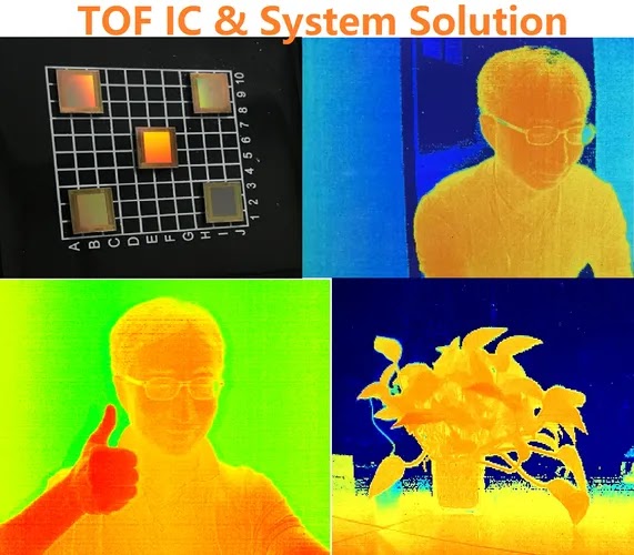
See Device Startup Proposes "Quantum PATPD Pixel"
July 17, 2019 By Leave a Comment
Image Sensors World Go to the original article...
Buena Park, CA-based See Device Inc. startup proposes:"Photon Assisted Tunneling Photodetector (PAT-PD) Technology, is new photodetector technology redefining what's possible with standard silicon CMOS image sensor without compromise to performance and efficiency. An innovative pixel array system formed by new structures and design mechanisms of silicon, SeeDevice's proprietary image sensor uses Quantum Tunneling resulting in high sensitivity, quantum efficiency, low SNR, and wide spectral response."

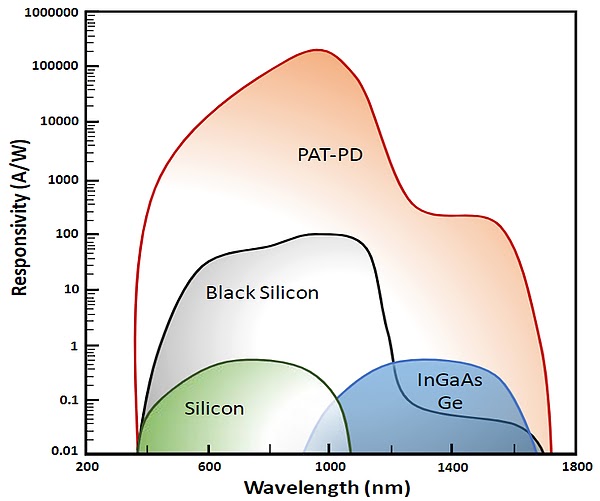

"The PAT-PD sensor is designed incorporating principles of quantum mechanics and nanotechnology to produce groundbreaking improvements in dynamic range, sensitivity, and low light capabilities without compromising size and efficiency. Standard sensors require conceding either the cost efficiency of CMOS and the better specifications of CCD sensors. This compromise is eliminated by the groundbreaking technology used in the SeeDevice image sensors and photodetectors.
PAT-PD completely redefines the physical principles used for sensors by using photon-activated current flow. SeeDevice owns 50 patents worldwide which enable us to produce industry-disrupting specifications by using photons as a trigger mechanism to enable current flow. The technology has a wide spectrum of applications and can be easily integrated since the entire device is built on a CMOS process.
PAT-PD enables device development with no compromise on technical specification. One device can have high resolution, high frame rate, high sensitivity, and a wide dynamic range without modifications."

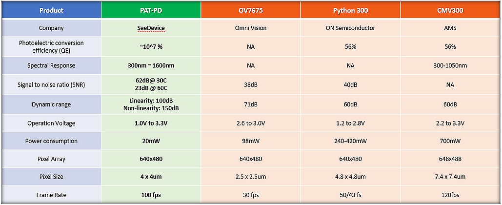

I'm told that the registered agent of Pixel Device Inc, Hoon Kim, has the same name as the CTO of infamous Planet82 company. Does anybody know if this is the same person?
Thanks to RA for the link!
Goodix Sues Egis over Under-Display Fingerprint Patents Infringement
July 16, 2019 By Leave a Comment
Image Sensors World Go to the original article...
Digitimes: China-based Goodix sues Taiwan's Egis Technology over infringing on its patents of under-display optical fingerprint sensors. Goodix sensors are used in many smartphones manufactured in China, while Egis sensors are used mostly in Samsung smartphones. The lawsuit was filed in Beijing IP court. Goodix demands CNY50.5M (US$7.35M) in compensation from Egis."With five years of arduous, tireless and indigenous innovation, a dedicated R&D team of 400+ overcame great difficulties to bring to the world the innovative optical IN-DISPLAY FINGERRPINT SENSOR, which has been leading a technological trend in the global mobile industry since its debut in early 2017. As of today, the innovative technology has been adopted by 52 smartphone models offered by mainstream brands, benefiting hundreds of millions of worldwide consumers, and is recognized as the most popular biometric solution in the bezel-less era.
The precious achievement is a result of enormous investment and persistence – Goodix invests at least 10% of its revenue into research and development each year. In 2018, the number has reached 22.5%, with a compound growth rate of 80% in the past five years. As of June, 2019, Goodix had submitted over 3,300 patent filings and accumulated over 480 issued patents, among which, over 760 filings and 50 issued patents are parts of the optical IN-DISPLAY FINGERPRINT SENSOR technology.
The success of Goodix’s optical IN-DISPLAY FINGERPRINT SENSOR embodies the hard work of all employees of Goodix; yet the team’s painstaking effort was stolen by a competitor. IP theft is a disrespectful act towards enterprises that are dedicated to innovations. It is also a vandalism of the market order. Out of the responsibilities and accountabilities to the employees, customers, consumers, as well as the entire industry, Goodix will defend its legitimate rights and interests by the justice of law.
Together with industry partners and peers, Goodix Technology is looking forward to establishing a healthy and sustainable industry environment that respects innovations and intellectual property rights."
Last year, Goodix was involved in a couple of lawsuits on capacitive fingerprint sensors. Goodix sued its Chinese competitor Silead, while Goodix itself was sued by Sweden-based FCP. This year, the optical fingerprint sensors are becoming a field of legal battles.


ADI Presents ToF Development Kit
July 16, 2019 By Leave a Comment
Image Sensors World Go to the original article...
Analog Devices presents its VGA ToF camera kit developed in cooperation with Arrow. The kit uses Panasonic CCD as a ToF sensor:
SPAD LiDAR from Chinese Academy of Science
July 16, 2019 By Leave a Comment
Image Sensors World Go to the original article...
Acta Photonics Sinica publishes a paper "A 16×1 Pixels 180nm CMOS SPAD-based TOF Image Sensor for LiDAR Applications" by CAO Jing, ZHANG Zhao, QINan, LIU Li-yuan, and WU Nan-jian."The sensor integrates 16 structure-optimized single photon avalanche diode pixels and a dual-counter-based 13-bit time-to-digital converter. Each pixel unit has a novel active quench and recharge circuit. The dark noise of single photon avalanche diode is reduced by optimizing the guard ring of the device. The active quench and recharge circuit with a feedback loop is proposed to reduce the dead time. A dual-counter-based time-to-digital converter is designed to prevent counting errors caused by the metastability of the counter in the time-to-digital converter. The sensor is fabricated in 180 nm CMOS standard technology. The measurement results show the median dark count rate of the single photon avalanche diode is 8 kHz at 1 V excess voltage, the highest photon detection efficiency is 18% at 550 nm light wavelength. The novel active quench circuit effectively reduces the dead time down to 8 ns. The time-to-digital converter with 416 ps resolution makes the system achieve the centimeter-accuracy detection. A 320×160 depth image is captured at a distance of 0.5 m. The maximum depth measurement nonlinear error is 1.9% and the worst-case precision is 3.8%."


TrinamiX Presents 3D FaceID Module
July 15, 2019 By Leave a Comment
Image Sensors World Go to the original article...
LinkedIn: TrinamiX unveils its compact FaceID solution for smartphones: "Protecting your data is nowadays more important than ever. #trinamiX3Dimaging allows you to protect your confidential infos by unlocking your mobile device only by facial recognition.The system does not only provide 2D and 3D information, but also a material classification which adds another authentication layer: skin recognition is introduced as a further protective barrier. The #3DImager thus enhances the #safety of mobile devices.
See in the picture below the 3D Imaging system for mobile applications."


Trinamix also demos its fiber-based distance measuring system for industrial applications:
Samsung Event-Driven Sensors
July 15, 2019 By Leave a Comment
Image Sensors World Go to the original article...
Hyunsurk Eric Ryu from Samsung presents the company's progress with event-driven sensors:Sony FE 50mm f1.4 ZA review
July 15, 2019 By Leave a Comment
Cameralabs Go to the original article...
The Sony FE 50mm f1.4 ZA is a standard prime lens designed for Sony's E-mount mirrorless cameras and corrected for full-frame bodies. It’s Sony’s top-end option with Zeiss optics and a fast f1.4 focal ratio. Find out how it compares to the other options in Thomas’s full review!…
The post Sony FE 50mm f1.4 ZA review appeared first on Cameralabs.
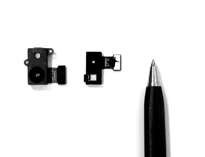
Melexis ToF Sensor Detailed Datasheet
July 15, 2019 By Leave a Comment
Image Sensors World Go to the original article...
Melexis publishes quite a detailed datasheet of its MLX75024 QVGA ToF sensor based on Sony-Softkinetic pixel. So detailed spec is quite a rarity in the world of ToF imaging:


Passive Image Recognition
July 14, 2019 By Leave a Comment
Image Sensors World Go to the original article...
University of Wisconsin-Madison publishes OSA Photonics Research paper "Nanophotonic media for artificial neural inference" by Erfan Khoram, Ang Chen, Dianjing Liu, Lei Ying, Qiqi Wang, Ming Yuan, and Zongfu Yu proposes a glass that performs NN taks:"Now, artificial intelligence gobbles up substantial computational resources (and battery life) every time you glance at your phone to unlock it with face ID. In the future, one piece of glass could recognize your face without using any power at all.
“This is completely different from the typical route to machine vision,” says [Zongfu] Yu.
He envisions pieces of glass that look like translucent squares. Tiny strategically placed bubbles and impurities embedded within the glass would bend light in specific ways to differentiate among different images. That’s the artificial intelligence in action.
For their proof of concept, the engineers devised a method to make glass pieces that identified handwritten numbers. Light emanating from an image of a number enters at one end of the glass, and then focuses to one of nine specific spots on the other side, each corresponding to individual digits.
The glass was dynamic enough to detect, in real-time, when a handwritten 3 was altered to become an 8.
Designing the glass to recognize numbers was similar to a machine-learning training process, except that the engineers “trained” an analog material instead of digital codes. Specifically, the engineers placed air bubbles of different sizes and shapes as well as small pieces of light-absorbing materials like graphene at specific locations inside the glass.
“We could potentially use the glass as a biometric lock, tuned to recognize only one person’s face” says Yu. “Once built, it would last forever without needing power or internet, meaning it could keep something safe for you even after thousands of years.”
My only concern is that the high optical power needed for non-linear operations in "NN glass" might burn the person's face. However, if recognition is achieved in nanosecond time with a short laser pulse, this might not be an issue:


Luminar Raises $100M More
July 13, 2019 By Leave a Comment
Image Sensors World Go to the original article...
BusinessWire, Venturebeat, Techcrunch, Wired: A 1550nm mechanical galvo mirror scanning LiDAR startup Luminar announces $100M funding round that brings its total raised capital to $250M and its valuation to $900M. Other than existing investors, G2VP, Crescent Cove Advisors, Octave Ventures, Moore Strategic Ventures, the Westly Group, 1517 Fund, Peter Thiel’s investment group, GoPro founder Nick Woodman, and strategic backers Corning Inc., Cornes, and Volvo Cars Tech Fund have joined the round. Cornes will support Luminar’s expansion into Asia, while Corning will codevelop auto-grade and lidar-friendly Gorilla Glass windows and other components.Luminar announces its new fully automotive qualified platform called Iris. It will be offered in two versions when it becomes available later this year. The higher end one costs $1,000 in production quantities and enable hands-free “freeway autonomy,” while the cheaper ADAS version costing under $500 will drive functions like emergency braking and steering.
The company says that it’s currently quoting and in the process of arranging multi-year contracts worth more than $1.5b combined.
Iris platform is said to be capable of seeing objects at 250m distance while consuming 15W of power.


SQUAD 2019 – Advanced School on Quantum Detectors
July 12, 2019 By Leave a Comment
Image Sensors World Go to the original article...
FBK and the University of Trento are organizing a school for PhD students and young researchers on Quantum detectors. Among the speakers, there will be many experts in single-photon imaging.SQUAD 2019, the Advanced School on Quantum Detectors, is to be held in Fondazione Bruno Kessler at its Science and Technology Hub in Povo, on the suburban hills of Trento, Italy, on September 18-20, 2019.
The preliminary program is quite impressive:
- Single photons in quantum mechanics: more than clicks on detectors
Prof. André Stefanov, University of Bern (Switzerland) - Waveguide integrated superconducting single photon detectors
Prof. Wolfram Pernice, University of Münster (Germany) - Fundamentals of single-photon avalanche diodes
Prof. Angelo Gulinatti, Politecnico di Milano (Italy) - Silicon photo-multipliers
Dr. Fabio Acerbi, Fondazione Bruno Kessler (Italy) - CMOS SPADs for single photon imaging [title TBC]
Dr. Sara Pellegrini, ST Microlectronics (United Kingdom) - Vacuum photodetectors [title TBC]
Dr. Serge Duarte Pinto, Photonis (The Netherlands) - Quantum imaging using Timepix3-based optical cameras [title TBC]
Dr. Andrei Nomerotski, Brookhaven National Laboratory (U.S.A.) - Cryo-CMOS for quantum applications
Prof. Edoardo Charbon, Ecole Polytechnique Fédérale de Lausanne (Switzerland) - Imaging technologies for quantum applications
Dr. Colin Coates, Andor (United Kingdom) - Past and future uses of single-photon detectors [title TBC]
Dr. Gianluca Boso, ID Quantique SA (Switzerland) - Can science benefit from advances in consumer electronics? [title TBC]
Dr. Robert Kappel, ams (Switzerland) - Applications in computational and quantum imaging using SPAD/emCCD sensors
Prof. Daniele Faccio, University of Glasgow (United Kingdom) - Validation of échelle-based quantum-classical discriminator with novelty SPAD array sensor
Dr. Dmitri Boiko, CSEM (Switzerland)

ON Semi HDR with LFM Promotional Video
July 12, 2019 By Leave a Comment
Image Sensors World Go to the original article...
ON Semi publishes a video promoting its HDR with LFM automotive image sensors:Daguerreotypes as Early Plasmonic Imagers
July 11, 2019 By Leave a Comment
Image Sensors World Go to the original article...
Proceedings of the National Academy of Sciences publishes a commentary "Plasmonics sheds light on the nanotechnology of daguerreotypes" by Naomi J. Halas on open-access paper "Nineteenth-century nanotechnology: The plasmonic properties of daguerreotypes" by Andrea E. Schlather, Paul Gieri, Mike Robinson, Silvia A. Centeno, and Alejandro Manjavacas talks about a newly found explanation of daguerreotype imaging:"...before plasmonic nanostructures became a science, they were an art. The invention of the daguerreotype was publicly announced in 1839 and is recognized as the earliest photographic technology that successfully captured an image from a camera, with resolution and clarity that remain impressive even by today’s standards. Here, using a unique combination of daguerreotype artistry and expertise, experimental nanoscale surface analysis, and electromagnetic simulations, we perform a comprehensive analysis of the plasmonic properties of these early photographs, which can be recognized as an example of plasmonic color printing."


Sigma 35mm f1.2 Art review
July 11, 2019 By Leave a Comment
Cameralabs Go to the original article...
The Sigma 35mm f1.2 DG DN Art is a mild wide-angle lens designed for full-frame mirrorless cameras and available in the Sony E and Leica L mounts, the latter working on Leica, Panasonic and Sigma L-mount bodies. The brightest 35mm lens with autofocus to date, it delivers attractive bokeh and impressive sharpness. Find out why you'll want it in our review!…
The post Sigma 35mm f1.2 Art review appeared first on Cameralabs.
UTAC Automotive Sensor Packages
July 11, 2019 By Leave a Comment
Image Sensors World Go to the original article...
UTAC paper "CMOS Image Sensor Packaging Technology for Automotive Applications" by Teoh Eng Kang, Alastair Attard, and Jonathan Abela says "Whereas high reliability image sensor packages are typically based on ceramic packages, these tend to have considerably higher costs and longer development cycles than laminate-based packages which are normally used in other market segments. In this paper, we present novel methods for packaging image sensors on laminate substrates, enabling a reduction in cost, form factor and time-to-market whilst simultaneously meeting automotive reliability grades typically required for such devices."


TechInsights Overviews Smartphone CIS Advances: Chip-stacking and Chip-to-chip Interconnect
July 10, 2019 By Leave a Comment
Image Sensors World Go to the original article...
TechInsights starts publishing a series of blog posts "The State-of-the-Art of Smartphone Imagers" based on Ray Fontaine's presentation at IISW 2019 at the end of June. The first part talks about chip-stacking and chip-to-chip interconnect:"A brief history of stacked smartphone imagers from three leaders is illustrated as follows. Sony launched its first stacked chips with dual TSVs and evolved to a single TSV structure. Its first generation 6 µm pitch Cu-Cu hybrid bonding is still in wide use however we’ve just documented in 2019 an evolution to 3.1 µm pitch Cu-Cu hybrid bonding in its 0.8 µm pixel generation sensor. To our knowledge this is the world record for imager Cu-Cu hybrid bonding pitch. OmniVision and foundry partners have produced butted TSV, single TSV and Cu-Cu direct hybrid bond interconnects. To our knowledge, TSMC holds the world record for imager single TSV pitch at 4.0 µm. W-filled TSVs are the preferred interconnect choice for Samsung stacked imagers and we’ve documented 5.0 µm TSVs in its stacked imagers."


Digitimes: 3D Sensing Market Surge Expected
July 10, 2019 By Leave a Comment
Image Sensors World Go to the original article...
Digitimes article "Taiwan chipmakers gearing up for 3D sensor market boom" quotes foundries Win Semiconductors and Advanced Wireless Semiconductor (AWSC), epitaxial wafer supplier Visual Photonics Epitaxy (VPEC), Himax, and backend houses ChipMOS Technologies, Xintec, and ShunSin Technology expecting imminent rise in 3D sensing orders for smartphones and ADAS.Win Semi sees orders for ToF components ramping up from Apple suppliers and also non-Apple customers. VPEC provides epi-wafers for Samsung ToF VCSELs as well as being a major epi-wafer source for Win Semi. AWSC sees increased orders form Ams. ChipMOS gets 3D sensing orders from Himax, ShunSin gets 3D orders from its parent company Foxconn.
Valeo Reports $564M in Design Wins for its LiDAR
July 9, 2019 By Leave a Comment
Image Sensors World Go to the original article...
Reuters: Valeo has won 500M euros ($564M) worth of orders for automotive LiDARs, told Valeo CEO Marc Vrecko in an interview, highlighting the potential growth of LiDAR. “Those 500 million euros of orders with four major global auto groups will probably eventually represent between 1 to 1.5 billion worth of recurring business,” said Vrecko. Valeo SCALA LiDAR is re-branded version of German Ibeo product.More than $1b in corporate and private investment has gone into some 50 LiDAR startups over the past three years, including a record $420M in 2018, according to a Reuters analysis of publicly available investment data in March.

SiOnyx Announces a Cheaper Vesrion of its Black Silicon Sensor Camera
July 9, 2019 By Leave a Comment
Image Sensors World Go to the original article...
BusinessWire: SiOnyx launches a cheaper version of its Aurora color night vision camera: "the new SiOnyx Aurora Sport HD action video camera for an introductory price of just $399. Unveiled at ICAST, the Sport uses SiOnyx’s proprietary Ultra Low Light imaging to turn night into full-color daylight. This imaging is the same semiconductor technology that earned the company a $20 million contract with the US Army."“As we continue to advance our black silicon technology for the law enforcement and defense industries, we are thrilled to expand our product offerings and bring that same expertise to the recreational market,” said Stephen Saylor, CEO of SiOnyx.

Sony FE 35mm f1.8 review
July 9, 2019 By Leave a Comment
Cameralabs Go to the original article...
The Sony FE 35mm f1.8 is a mild wide-angle prime lens for its Alpha mirrorless cameras. It’s Sony’s third native 35mm lens that’s corrected for full-frame bodies, but pitched at a more affordable price and similar in build and quality to the FE 85mm f1.8. Find out why it's a great option for the money in out full review!…
The post Sony FE 35mm f1.8 review appeared first on Cameralabs.