Chronoptics compares depth sensing methods

Image Sensors World        Go to the original article...

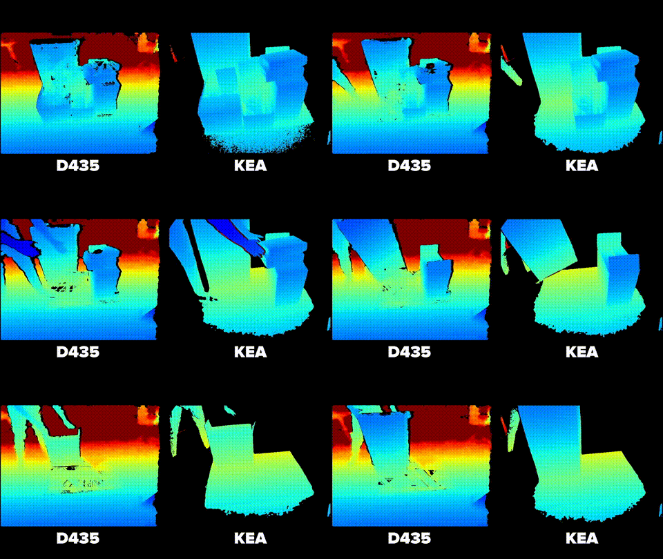
In a blog post titled "Comparing Depth Cameras: iToF Versus Active Stereo" Refael Whyte of Chronoptics compares depth reconstructions from their indirect time-of-flight (iToF) "KEA" camera with active stereo using an Intel RealSense D435 sensor.


Specs


Setup used for comparisons

Bin picking

Pallet picking


Depth data can also be overlaid on RGB to get colored point cloud visualizations. KEA provides much cleaner-looking results:

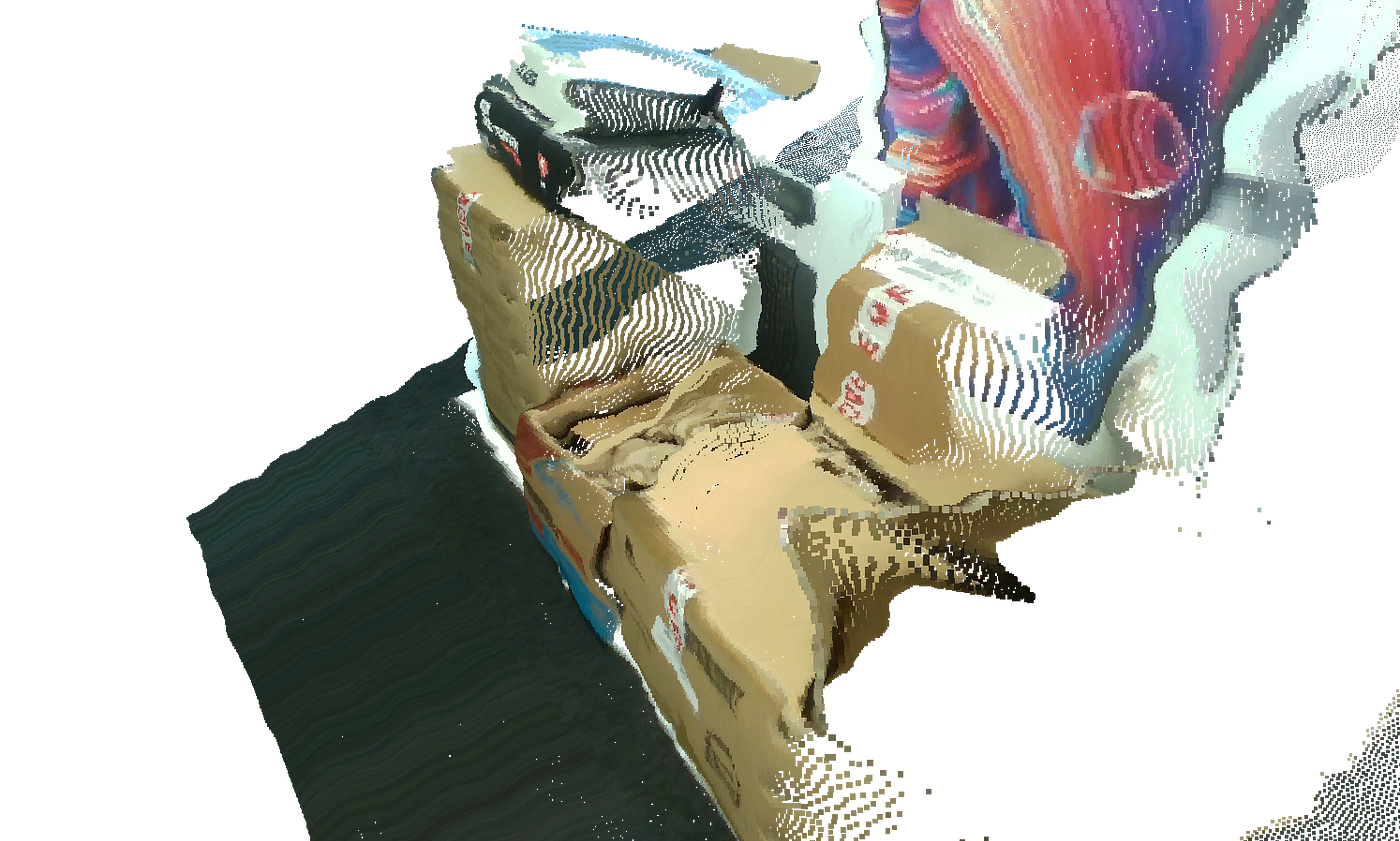
 
KEA


D435


They show some limitations too. In this scene the floor has very low reflectivity in IR so the KEA camera struggles to collect enough photons there:
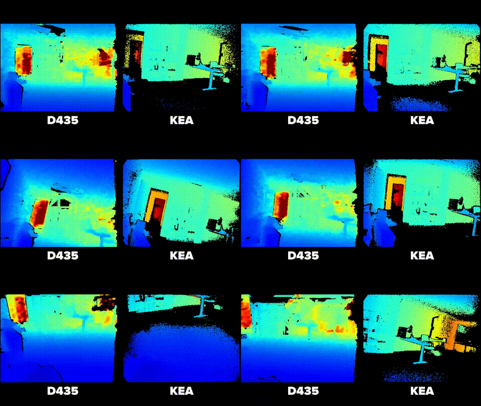


[PS: I wish all companies showed "failure cases" as part of their promotional materials!]

Full article here: https://medium.com/chronoptics-time-of-flight/comparing-depth-cameras-itof-versus-active-stereo-e163811f3ac8

Go to the original article...

BrainChip + Prophesee partnership

Image Sensors World        Go to the original article...


Laguna Hills, Calif. – June 14, 2022 – BrainChip Holdings Ltd (ASX: BRN, OTCQX: BRCHF, ADR: BCHPY), the world’s first commercial producer of neuromorphic AI IP, and Prophesee, the inventor of the world’s most advanced neuromorphic vision systems, today announced a technology partnership that delivers next-generation platforms for OEMs looking to integrate event-based vision systems with high levels of AI performance coupled with ultra-low power technologies.

Inspired by human vision, Prophesee’s technology uses a patented sensor design and AI algorithms that mimic the eye and brain to reveal what was invisible until now using standard frame-based technology. Prophesee’s computer vision systems open new potential in areas such as autonomous vehicles, industrial automation, IoT, security and surveillance, and AR/VR.

BrainChip’s first-to-market neuromorphic processor, Akida, mimics the human brain to analyze only essential sensor inputs at the point of acquisition, processing data with unparalleled efficiency, precision, and economy of energy. Keeping AI/ML local to the chip, independent of the cloud, also dramatically reduces latency.

“We’ve successfully ported the data from Prophesee’s neuromorphic-based camera sensor to process inference on Akida with impressive performance,” said Anil Mankar, Co-Founder and CDO of BrainChip. “This combination of intelligent vision sensors with Akida’s ability to process data with unparalleled efficiency, precision and economy of energy at the point of acquisition truly advances state-of-the-art AI enablement and offers manufacturers a ready-to-implement solution.”

“By combining our Metavision solution with Akida-based IP, we are better able to deliver a complete high-performance and ultra-low power solution to OEMs looking to leverage edge-based visual technologies as part of their product offerings, said Luca Verre, CEO and co-founder of Prophesee.”

For additional information about the BrainChip/Prophesee partnership contact sales@brainchip.com.

“We’ve successfully ported the data from Prophesee’s neuromorphic-based camera sensor to process inference on Akida with impressive performance,” said Anil Mankar, Co-Founder and CDO of BrainChip. “This combination of intelligent vision sensors with Akida’s ability to process data with unparalleled efficiency, precision and economy of energy at the point of acquisition truly advances state-of-the-art AI enablement and offers manufacturers a ready-to-implement solution.”

“By combining our Metavision solution with Akida-based IP, we are better able to deliver a complete high-performance and ultra-low power solution to OEMs looking to leverage edge-based visual technologies as part of their product offerings, said Luca Verre, CEO and co-founder of Prophesee.”

ABOUT BRAINCHIP HOLDINGS LTD (ASX: BRN, OTCQX: BRCHF, ADR: BCHPY)

BrainChip is the worldwide leader in edge AI on-chip processing and learning. The company’s first-to-market neuromorphic processor, AkidaTM, mimics the human brain to analyze only essential sensor inputs at the point of acquisition, processing data with unparalleled efficiency, precision, and economy of energy. Keeping machine learning local to the chip, independent of the cloud, also dramatically reduces latency while improving privacy and data security. In enabling effective edge compute to be universally deployable across real world applications such as connected cars, consumer electronics, and industrial IoT, BrainChip is proving that on-chip AI, close to the sensor, is the future, for its customers’ products, as well as the planet.

Explore the benefits of Essential AI at www.brainchip.com. 

For additional information about the BrainChip/Prophesee partnership, contact sales@brainchip.com.

ABOUT PROPHESEE

Prophesee is the inventor of the world’s most advanced neuromorphic vision systems.

The company developed a breakthrough Event-based Vision approach to machine vision. This new vision category allows for significant reductions of power, latency and data processing requirements to reveal what was invisible to traditional frame-based sensors until now. Prophesee’s patented Metavision® sensors and algorithms mimic how the human eye and brain work to dramatically improve efficiency in areas such as autonomous vehicles, industrial automation, IoT, security and surveillance, and AR/VR.

Prophesee is based in Paris, with local offices in Grenoble, Shanghai, Tokyo and Silicon Valley. The company is driven by a team of more than 100 visionary engineers, holds more than 50 international patents and is backed by leading international equity and corporate investors including 360 Capital Partners, European Investment Bank, iBionext, Intel Capital, Robert Bosch Ventures, Sinovation, Supernova Invest, Will Semiconductor, Xiaomi.

Go to the original article...

New image sensor in ARRI’s latest Alexa 35 cine camera

Image Sensors World        Go to the original article...

From NewsShooter: https://www.newsshooter.com/2022/06/01/arri-alexa-35-first-look/

ARRI has officially unveiled the ALEXA 35, a new Super 35 digital cinema camera with 17 stops of dynamic range and a host of new features that are all aimed to provide the best possible image quality.

The ALEXA 35 has big shoes to fill as it is the first ARRI camera to feature a sensor that isn’t based on the ALEV-III. The ALEV-III has been used in various forms in every single ALEXA camera since 2010. The ALEXA 35 represents the next big step for ARRI in the evolution of the ALEXA family.


With its new image sensor with ~6 micron pixel pitch, Arri claims to provide 17 stop of dynamic range but details about the sensor manufacturer were not available on their website. Earlier models of their camera used the Alev-III sensor which was a CMOS sensors from onsemi.

A couple of other videos about the new Alexa 35:


Go to the original article...

Recent Image Sensor Videos

Image Sensors World        Go to the original article...

Sony presents "Advantages of Large Format Global Shutter and Rolling Shutter Image Sensor"


onsemi presents their CMOS image sensor layer structure consisting of a microlens array, color filter array, photodiode, pixel transistors, bond layer and ASIC:


Newsight presents its enhanced time-of-flight technology for depth sensing:


And finally a cute cat video to wrap it up: Samsung's new 200 megapixel ISOCELL image sensor promotional video:


Go to the original article...

PhD Thesis on Dynamic Range Improvements

Image Sensors World        Go to the original article...

A PhD thesis titled "Proposal of Architecture and Circuits for Dynamic Range Enhancement of Vision Systems on Chip designed in Deep Submicron Technologies" by from Universidad de Sevilla is now available to the public. The thesis is by Sonia Vargas Sierra who did this work at the Image Sensor group of Microelectronic Institute of Seville.

Although the thesis is from a few years ago, some of the content in the thesis may be of interest now due to recent developments in vertical integrated technologies.

From the Preface:

The work presented in this thesis proposes new techniques for dynamic range expansion in electronic image sensors. Since Dynamic Range (DR) is defined as the ratio between the maximum and the minimum measurable illuminations, the options for improvement seem obvious; first, to reduce the minimum measurable signal by diminishing the noise floor of the sensor, and second, to increase the maximum measurable light by increasing the sensor saturation limit.

In our case, we focus our studies to the possibility of providing DR enhancement functionality in a single chip, without requiring any external software/hardware support, composing what is called a Vision-System-on-Chip (VSoC). In order to do so, this thesis covers two approaches. Chronologically, our first option to improve the DR relied on reducing the noise by using a fabrication technology that is specially devoted to image sensor fabrication, a so-called CMOS Image Sensor (CIS) technology. However, measurements from a test chip indicated that the dynamic range improvement was not sufficient to our purposes (beyond the 100dB limit). Additionally, the technology had some important limitations on what kind of circuitry can be placed next to the photosensor in order to improve its performance. Our second approach has consisted in, first, designing a tone mapping algorithm for DR expansion whose computational needs can be easily mapped onto simple signal conditioning and processing circuitry around the photosensor, and second, designing a test chip implementing this algorithm in a standard CMOS technology.

This thesis is organized in five chapters. Chapter 1 describes the main concepts involved in image sensors focusing in High Dynamic Range (HDR) operation. Chapter 2 presents the study of an image sensor optimized technology in order to be considered for dynamic range improvement techniques. Chapter 3 describes an innovative tone mapping algorithm used to optimize the compression of HDR scenes. Chapter 4 introduces the image sensor chip that has been designed and fabricated, which implements the new tone mapping algorithm. Chapter 5 shows the experimental results and evaluation of the performance of the chip. 


Link to download thesis pdf: https://idus.us.es/handle/11441/130619


A couple of references related to the topic of this thesis: 
  1. S. Vargas-Sierra et al., "A 151 dB high dynamic range CMOS image sensor chip architecture with tone mapping compression embedded in-pixel", IEEE Sensors J. Jan. 2015. https://ieeexplore.ieee.org/document/6860247 
  2. Mori et al., "A 4.0 μm Stacked Digital Pixel Sensor Operating in a Dual Quantization Mode for High Dynamic Range," IEEE TED June 2022 issue. https://ieeexplore.ieee.org/abstract/document/9762367/

Go to the original article...

Evolution of Image Sensor Architectures With Stacked Device Technologies (IEEE TED June 2022)

Image Sensors World        Go to the original article...

In a paper titled "Evolution of Image Sensor Architectures With Stacked Device Technologies" in IEEE TED (June 2022) Y. Oike writes:

The evolution of CMOS image sensors and their prospects using advanced imaging technologies are promising candidates to improve the quality of life. With the rapid advent of parallel analog-to-digital converters (ADCs) and back-illuminated (BI) technology, CMOS image sensors currently dominate the market for digital cameras, and stacked CMOS image sensors continue to provide enhanced functionality and user experience in mobile devices. This article reviews the latest achievements in stacked image sensors with respect to the evolution of image sensor architecture for accelerating performance improvements, extending sensing capabilities, and integrating edge computing with various stacked device technologies.


[IEEE subscription required]

Go to the original article...

AlpsenTek vision sensor startup raises nearly $30 million

Image Sensors World        Go to the original article...

Chinese vision sensor startup AlpsenTek raised nearly $30 million in Series A funding

AlpsenTek(锐思智芯), a Chinese machine vision sensor startup, announced on June 6 that it raised nearly RMB200 million($30 million) in Series A funding earlier this year.

The investment was was jointly led by Xunxing Investment - an investment company of Chinese smartphone brand OPPO and Cowin Capital.  


AlpsenTek’s original investors ArcSoft Corp, Sunny Optical Industry Fund, Clory Ventures, Shenzhen Angel FOF, Lenovo Capital and Incubator Group, and Zero2IPO Group also participated in this round of funding.  

Founded in 2019, AlpsenTek is a company engaged in the research and development of machine vision sensors and algorithms. The company is headquartered in Beijing and has offices in Shenzhen, Nanjing, and Switzerland.

AlpsenTek employs an international team of professionals from elite research firms worldwide with extensive expertise in developing algorithms, software, hardware, and chips, according to the company.

The core products of AlpsenTek are the ALPIX series hybrid biomimetic vision chips and integrated machine vision solutions. The company said that it holds a complete core set of intellectual property rights and in-house development capabilities to fill technology gaps in machine vision. The company also has begun to cooperate with leading players in the industry. Its products can be widely used in robots, smartphones, unmanned driving, drones, security, and other fields, with a potential market size of over RMB1 trillion ($150 billion).

Original article: https://jw.ijiwei.com/n/821276

Go to the original article...

Smartphone imaging trends webinar and whitepaper

Image Sensors World        Go to the original article...

From Counterpoint Research (https://www.youtube.com/watch?v=veC5PS8aDZo):

Over the last few years, steady upgrades in CMOS image sensor (CIS) technology combined with the evolution of chipsets – and the improvements in AI they enable – are bringing step-change improvements to smartphone camera performance.

Counterpoint Research would like to invite you to join our latest webinar Smartphone Imaging Trends: New Directions Capturing Magic Moments which will be attended by key executives from HONOR, Qualcomm, and DXOMARK as well as a renowned professional photographer and director Eugenio Recuenco.

The webinar is a complement to an upcoming Counterpoint Whitepaper (also to be released on June 8) which will cover smartphone imaging trends, OEM strategy comparisons, the key components of a great camera and show how technology is helping to unlock creative expression.


The accompanying whitepaper can be obtained here: https://www.counterpointresearch.com/whitepaper-smartphone-imaging-trends/

The camera has always been a major component of the smartphone and a key selling point among consumers. In the past, smartphone cameras lagged far behind even the most basic DSLRs as form factor and size constraints impacted picture and video quality. But technology has now advanced to the point where today’s top flagship devices are capable of delivering DSLR-like performance.

The rise of AI algorithms, advancements in multi-frame/multi-lens computational photography, more powerful processors, the addition of dedicated image signal and neural processing units and, of course, the compounding of R&D experience has resulted in today’s smartphone cameras rivalling dedicated imaging devices.

In fact, the smartphone’s comparatively compact form factor is an advantage, as clicking pictures and recording videos are becoming integrated into our daily lives through the growth of social media. The role of the camera has shifted to become a life tool, as end-users migrate from being simply consumers of content to creators.

This new direction that imaging has taken warrants further advancements in smartphone cameras, as we lean on technology to make the experience easier while allowing all of us to be more creative.

Table of Contents:

Introduction
Smartphone Imaging Trends
Megapixels: More is not necessarily better
Multi-camera modules: Covering all scenarios
Image processing: Pushing the laws of physics
OEM Imaging Comparisons
As hardware slows, innovation grows
Where the magic happens
New magic, new directions
Measuring Quality
Components of an exceptional smartphone camera
Image processing innovation
DXOMARK Readout
Capturing Magic Moments
Powering art through technology
Conclusion


Go to the original article...

Lucid Vision Labs discusses EMVA 1288 specs for Sony IMX492

Image Sensors World        Go to the original article...

Lucid Vision Labs has released a new video overview of Sony's rolling shutter 47MP IMX492 sensor.


The video discusses quantum efficiency (time stamp 2:02), saturation capacity (3:04), temporal dark noise (3:15), and dynamic range (3:27). It also compares it to some of other higher resolution sensors (31.4MP IMX342, 24.5MP IMX530, 20MP IMX183)


Full EMVA 1288 data is also available on Lucid's product page under the "EMVA 1288 Data" Tab here: https://thinklucid.com/product/atlas10-47mp-imx492/#tab-emva-1288-data


Go to the original article...

Vayyar Raises Series-E

Image Sensors World        Go to the original article...

From TechCrunch:

Vayyar, a company developing radar-imaging sensor technologies, today announced that it raised $108 million in a Series E round led by Koch Disruptive Technologies, with participation from GLy Capital Management, Atreides Management LP, KDT, Battery Ventures, Bessemer Ventures, More VC, Regal Four and Claltech. The round brings Vayyar’s total raised to over $300 million, which CEO Raviv Melamed said is being put toward expanding across verticals and introducing a “family” of machine learning-powered sensor solutions for robotics, retail, public safety and “smart” building products.

“We are pleased and proud to progress our partnership with existing investors including KDT, as well as additional backers which are joining forces with us for the first time,” Melamed said in a statement. “During a challenging period for the global economy, this new funding round is a ringing endorsement of our mission and a clear vote of confidence in the strength of our technology and the strategic agility of our organization.”

Founded in 2011 by Miri Ratner, Naftali Chayat and Melamed, who was previously VP of Intel’s architecture group, Vayyar initially developed its sensor technology to provide an alternative means of screening for early-stage breast cancer. Leveraging MIMO antennas, short for “multiple input, multiple output,” Vayyar’s products can deliver a high-resolution mapping of their surroundings by sending and receiving signals from dozens of antennas.

Vayyar later expanded its “radar-on-chip” technology from healthtech to a number of other sectors, including automotive, senior care, retail, smart home and commercial property. Vayyar sells Vayyar Care, a fall detection system for monitoring people at higher risk of tripping and falling in bedrooms, bathrooms and other living spaces. In the automotive industry, Vayyar offers solutions for collision warnings, parking assistance, adaptive cruise control, seatbelt detection and automatic breaking. And in construction, Vayyar provides a handheld sensor called Walabot for detecting leaky pipes behind walls.

Vayyar competes with Entropix, Photonic Vision, Noitom Technology, Aquifi and ADI, among others, which offer their own flavors of MIMO-based sensors. But the company has long asserted that its software and algorithms set it apart from the competition. Evidently, they were impressive enough to convince Amazon to partner with Vayyar for fall detection on Alexa Together, a subscription service that remotely monitors and assists family members in their homes.

In recent years, Vayyar has entered into customer relationships with brands like Piaggio Group, which will deploy Vayyar’s sensors on some of its forthcoming motorbikes. The company also claims to have supply contracts with automakers from Japan and Vietnam as well as a joint venture agreement with Haier subsidiary HCH Ventures to leverage the latter’s “senior care technology” in China-based businesses.

Signaling ambitions in the Asia-Pacific market in particular, Vayyar noted in a press release that it engaged China International Capital Corporation Limited, a Beijing-based investment company, as its lead financial adviser for the Series E explicitly to “support investor outreach in China.” (One of Vayyar’s newer offices is in China.) Somewhat unusually, Vayyar’s Series E came just under its Seres D, which totaled $109 million. It’s unclear whether the valuation has changed — TechCrunch last reported that Vayyar was valued “north” of $600 million. 


https://techcrunch.com/2022/06/06/imaging-sensor-startup-vayyar-lands-108m-to-fuel-expansion/

Go to the original article...

In the News: Yole Webcast, Prophesee Software Suite

Image Sensors World        Go to the original article...

The CIS market is back to strong growth: Are we at the beginning of the much-awaited sensing era?

Yole will host a webcast on Thursday 16, June 2022


The image sensor market struggled through a mixed 2021 but appears to have emerged strongly positioned. Could 2022 be the beginning of strong growth on the back of sensing applications?
In this webcast we will explore what the next few quarters and years hold for the CMOS image sensor (CIS) industry, including market demand, industry revenue and capacity.

This webcast will take a quick look back at 2021 to review the recent history of CIS before focusing on the near and mid-term prospects for the CIS industry. It will also cover market dynamics, supply, and pricing, with particular focus on answering the question, “Are we at the beginning of strong growth on the back of sensing applications?”

Prophesee releases its entire event-based vision software suite for free, including commercial license, further enabling community of thousands of Engineers and Researchers Worldwide


New release of 5X award-winning suite includes a complete set of Machine Learning tools, new key Open-Source modules, ready-to-use applications, code samples and allows for completely free evaluation, development and release of products with the included commercial license.

With this advanced toolkit, engineers can easily develop computer vision applications on a PC for a wide range of markets, including industrial automation, IoT, surveillance, mobile, medical, automotive and more.

“We have seen a significant increase in interest and use of Event-Based Vision and we now have an active and fast-growing community of more than 4,500 inventors using Metavision Intelligence since its launch. As we are opening the event-based vision market across many segments, we decided to boost the adoption of MIS throughout the ecosystem targeting 40,000 users in the next two years. By offering these development aids, we can accelerate the evolution of event-based vision to a broader range of applications and use cases and allow for each player in the chain to add its own value,” said Luca Verre, co-founder and CEO of Prophesee.


Go to the original article...

Camera Arrays for Large Scale Surveillance

Image Sensors World        Go to the original article...

From the journal Light Science and Applications, in a paper titled "A modular hierarchical array camera" X. Yuan et al. write:

Abstract: Array cameras removed the optical limitations of a single camera and paved the way for high-performance imaging via the combination of micro-cameras and computation to fuse multiple aperture images. However, existing solutions use dense arrays of cameras that require laborious calibration and lack flexibility and practicality. Inspired by the cognition function principle of the human brain, we develop an unstructured array camera system that adopts a hierarchical modular design with multiscale hybrid cameras composing different modules. Intelligent computations are designed to collaboratively operate along both intra- and intermodule pathways. This system can adaptively allocate imagery resources to dramatically reduce the hardware cost and possesses unprecedented flexibility, robustness, and versatility. Large scenes of real-world data were acquired to perform human-centric studies for the assessment of human behaviours at the individual level and crowd behaviours at the population level requiring high-resolution long-term monitoring of dynamic wide-area scenes.


Given the potential applications shown (large scale surveillance), it is quite intriguing that the "Ethics Declaration" section of this paper is empty.

Open access link: https://www.nature.com/articles/s41377-021-00485-x

See also: https://image-sensors-world.blogspot.com/2022/06/surveillance-market-and-smartsens.html

Go to the original article...

Sony Investor Relations Day 2022

Image Sensors World        Go to the original article...

Slides from the Imaging and Sensing Solutions Segment from Sony's Investor Relations day:


Go to the original article...

Review of Quanta Image Sensors for Ultralow-Light Imaging (IEEE TED June 2022)

Image Sensors World        Go to the original article...

[As mentioned in some recent comments on this blog, the latest (vol. 69 no. 6, June 2022) issue of IEEE Transactions on Electron Devices has many interesting papers related to image sensors. I will post summaries here in the coming days.]

In an invited paper in the June 2022 issue of IEEE TED, Jiaju Ma et al. write:

The quanta image sensor (QIS) is a photon counting image sensor that has been implemented using different electron devices, including impact ionization gain devices, such as the single-photon avalanche detectors (SPADs), and low-capacitance, high conversion-gain devices, such as modified CMOS image sensors (CIS) with deep sub-electron read noise and/or low noise readout signal chains. This article primarily focuses on CIS QIS, but recent progress of both types is addressed. Signal processing progress, such as denoising, critical to improving apparent signal-to-noise ratio, is also reviewed as an enabling co-innovation.

https://ieeexplore.ieee.org/stamp/stamp.jsp?arnumber=9768129


Go to the original article...

Special Issue: Solid State Image Sensors on IEEE TED

Image Sensors World        Go to the original article...

My Friend Michael Guidash just informed me that the special issue for solid state image sensors on IEEE Transactions on Electron Devices in now available online.

Here is a link to the table of content: https://ieeexplore.ieee.org/stamp/stamp.jsp?tp=&arnumber=9780655

The list of papers can be found here: https://ieeexplore.ieee.org/xpl/mostRecentIssue.jsp?punumber=16 

Go to the original article...

Surveillance market and SmartSens

Image Sensors World        Go to the original article...

From DigiTimes Asia news: https://www.digitimes.com/news/a20220527PD203/sensor-surveillance.html


China security surveillance market boom buoys SmartSens

The expanding security surveillance market in China continues to boost the shipments of CMOS image sensor (CIS) chips from Chinese CIS startup SmartSens Technology, which has entered the supply chains of China's first-tier security camera vendors including Hikvision Digital Technology, Uniview Technologies and Dahua Technology, according to industry sources.

IDC statistics show China's security surveillance market scale reached US$16.2 billion in 2021 and is estimated to grow to US$20.1 billion in 2022, for a CAGR of 13.6% for the period. High-definition security camera lenses have become the tipping point of market growth, fast driving CIS sales in China, the sources said.

Since launching its first CIS chip SC1035 in 2014, SmartSens has quickly built a strong presence in the security surveillance sector. Its CIS shipments topped 100 million in 2017 and grew all the way to 146 million in 2020, registering the highest global market share at 35% in the security CIS sector, according to Frost & Sullivan statistics.

Over the years, SmartSens has been dedicated to developing high-performance CIS chips with higher light sensitivity and signal-to-noise ratios, as well as better low-light performance as the core requirements, while deepening deployments in AI, intelligent perception and machine vision capabilities, the industry sources noted.

In terms of future security-use CIS development, its co-founder and CEO Richard Xu has said that as the surveillance lens application scenarios continue to expand, the features of low light and wide dynamic range (WDR) will be increasingly highlighted for security camera solutions so that they can penetrate higher-end applications.

Since late April this year, SmartSens has kicked off a plan to list its shares on China's Sci-Tech Innovation Board (STAR Market), aiming to raise CNY2.82 billion to finance equipment procurement and system construction for its R&D center as well as the development of car-use CIS products, the sources said.

Go to the original article...

Growth in wafer capacity for image sensors

Image Sensors World        Go to the original article...

From Semiconductor Digest news: 

Global installed capacity for image sensors was one million 200mm-equivalent wafers per month at the end of 2021. According to the new Global Wafer Capacity 2022 report, image sensor capacity is forecast to increase 13% in 2022.


By the end of 2026, installed capacity for image sensors is projected to be 1.8 million 200mm-equiv. wafers per month. That’s an average annual growth rate of 12.5% over the forecast period, making image sensor capacity among the fastest growing segments.

While the Covid-19 pandemic negatively impacted the image sensor market in 2020, growth returned in 2021. Demand for digital imaging is increasing in virtually all areas, including cellphones, automotive, machine vision, security cameras, webcams, drones, and more.

While Sony in Japan is the industry’s leading CMOS image sensor supplier, the combined CIS capacity of Samsung and SK Hynix made Korea the industry’s biggest source for production of image sensors at the end of 2021.

More than a decade ago, Sony set a goal to become the largest supplier of image sensors for cellphones. After claiming the top spot, Sony in 2014 took aim at becoming the largest supplier of CMOS image sensors for automotive systems and it is pursuing machine vision applications in factory automation and drones as well as image-recognition security cameras. Sony also sells 3D imaging sensors for depth ranging, face recognition, artificial intelligence, and machine vision.


Sony was the first to manufacture image sensors on 300mm wafers. The company has continued expanding its CIS capacity by converting 300mm fabs from logic to image sensor production and by acquiring 300mm fabs from other companies in Japan looking to exit the business of fabricating ICs. Sony has eight 300mm fab lines at four sites in Japan, with the newest being Fab 5 in Nagasaki. Fab 5 started mass production in 2021 and the construction of an expansion is already underway.


Samsung entered the CMOS image sensor business to diversify its business beyond DRAM and NAND flash. Since the fabrication technologies and tool sets for CIS devices are like that of DRAM, Samsung repurposed older DRAM fabs to begin making image sensors. The company became the industry’s second largest supplier of image sensors by serving most of the camera module needs of its huge cellphone business. Samsung’s image sensor production exists primarily at a large 300mm fab facility in Hawseong, South Korea.

SK Hynix has used the same strategy of turning older DRAM fabs into capacity for CMOS image sensors but lacks the benefit of having another related SK Hynix operation to buy its CIS devices. The company has a small but growing share of the global image sensor market.

The industry’s third largest supplier of image sensors is OmniVision but it relies on external foundries for the fabrication of its CIS wafers. OmniVision’s primary sources of foundry capacity are TSMC in Taiwan and SMIC and HLMC in China.

https://www.semiconductor-digest.com/strong-growth-in-wafer-capacity-for-image-sensors-expected/

Go to the original article...

Review article on photonics + deep learning

Image Sensors World        Go to the original article...

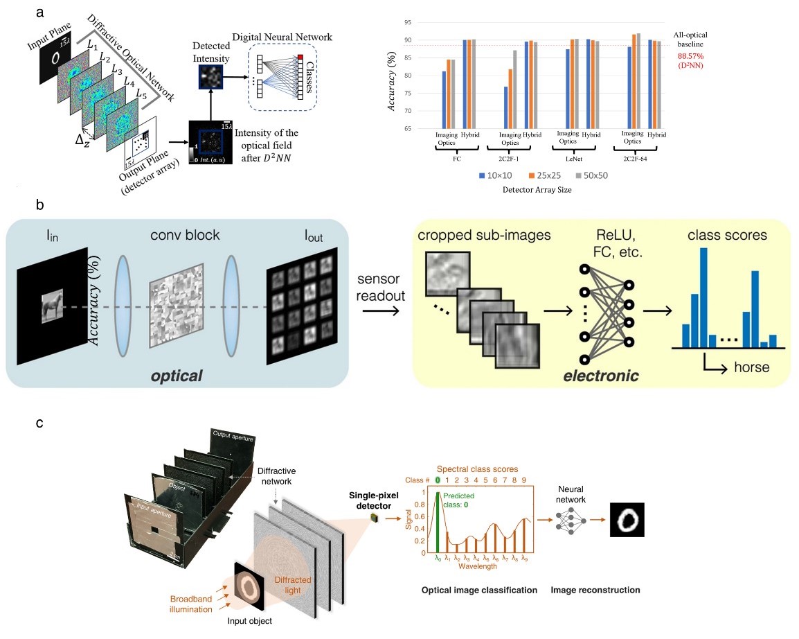
A team from UCLA has published a review article titled "At the intersection of optics and deep learning: statistical inference, computing, and inverse design" in Optica Advances in Optics and Photonics:

Deep learning has been revolutionizing information processing in many fields of science and engineering owing to the massively growing amounts of data and the advances in deep neural network architectures. As these neural networks are expanding their capabilities toward achieving state-of-the-art solutions for demanding statistical inference tasks in various applications, there appears to be a global need for low-power, scalable, and fast computing hardware beyond what existing electronic systems can offer. Optical computing might potentially address some of these needs with its inherent parallelism, power efficiency, and high speed. Recent advances in optical materials, fabrication, and optimization techniques have significantly enriched the design capabilities in optics and photonics, leading to various successful demonstrations of guided-wave and free-space computing hardware for accelerating machine learning tasks using light. In addition to statistical inference and computing, deep learning has also fundamentally affected the field of inverse optical/photonic design. The approximation power of deep neural networks has been utilized to develop optics/photonics systems with unique capabilities, all the way from nanoantenna design to end-to-end optimization of computational imaging and sensing systems. In this review, we attempt to provide a broad overview of the current state of this emerging symbiotic relationship between deep learning and optics/photonics.


https://opg.optica.org/aop/abstract.cfm?uri=aop-14-2-209

Go to the original article...

SmartSens Goes Public on Shanghai Stock Exchange

Image Sensors World        Go to the original article...

From PRNewsWire:


SHANGHAI, May 23, 2022 /PRNewswire/ -- On May 20, 2022, SmartSens was officially listed on the Science and Technology Innovation Board of the Shanghai Stock Exchange (Stock Code: 688213). On the first day of trading, SmartSens shares surged by 79.82%, with a total market value of 22.66 billion yuan.


SmartSens Technology (Shanghai) Co., Ltd. (Stock Code: 688213) is a high-performance CMOS image sensor (CIS) chip design company. It is headquartered in Shanghai and has research centers in many cities around the world.

SmartSens has been dedicated to pushing forward the frontier of imaging technology and growing in popularity among customers since it was established. SmartSens' CMOS image sensors provide advanced imaging solutions for a broad range of areas such as surveillance, machine vision, automotive and cellphone cameras.

SmartSens is committed to continuous innovation of products and fueling growth in numerous industries by delivering a more comprehensive portfolio of image sensors.

Go to the original article...

Preprint on unconventional cameras for automotive applications

Image Sensors World        Go to the original article...

From arXiv.org --- You Li et al. write:

Autonomous vehicles rely on perception systems to understand their surroundings for further navigation missions. Cameras are essential for perception systems due to the advantages of object detection and recognition provided by modern computer vision algorithms, comparing to other sensors, such as LiDARs and radars. However, limited by its inherent imaging principle, a standard RGB camera may perform poorly in a variety of adverse scenarios, including but not limited to: low illumination, high contrast, bad weather such as fog/rain/snow, etc. Meanwhile, estimating the 3D information from the 2D image detection is generally more difficult when compared to LiDARs or radars. Several new sensing technologies have emerged in recent years to address the limitations of conventional RGB cameras. In this paper, we review the principles of four novel image sensors: infrared cameras, range-gated cameras, polarization cameras, and event cameras. Their comparative advantages, existing or potential applications, and corresponding data processing algorithms are all presented in a systematic manner. We expect that this study will assist practitioners in the autonomous driving society with new perspectives and insights.


Go to the original article...

Single Photon Workshop 2022 – Call for Papers

Image Sensors World        Go to the original article...

After a short hiatus, Single Photon Workshop will be held in person from October 31 to November 4, 2022 at the Korea Institute of Science and Technology (KIST) in Seoul, South Korea.


SPW 2022 is the tenth and latest installment in a series of biennial workshops on single-photon technologies and applications. After one-year delay due to COVID-19, SPW 2022 is intended to bring together again a broad range of people with interests in single-photon sources, single-photon detectors, photonic quantum metrology, and their applications such as quantum information processing. Researchers from universities, industry, and government will present their latest developments in single-photon devices and methods with a view toward improved performance and new application areas. It will be an exciting opportunity for those interested in single-photon technologies to learn about the state-of-the-art and to foster continuing partnerships with others seeking to advance the capabilities of such technologies.

1-page abstract submissions are now being accepted on various topics (see table below). Submission period is from Apr 25 - July 1, 2022.


The KIST campus is located in the northeast side of Seoul and can be easily reached by subway from anywhere in Seoul and near Seoul. The presentation room would be Johnson Auditorium in Building A1 with a seating capacity of 420 people. For poster presentation and exhibition, an open space in the 1st floor in L3 would be reserved.

Visit http://spw2022.org/ for more information.

Go to the original article...

PreAct and Espros working on new lidar solutions

Image Sensors World        Go to the original article...

From optics.org news:

PreAct Technologies, an Oregon-based developer of near-field flash lidar technology and Espros Photonics, Sargans, Switzerland, a firm producing time-of flight chips and 3D cameras, have announced a collaboration agreement to develop new flash lidar technologies for specific use cases in automotive, trucking, industrial automation and robotics.

The collaboration combines the dynamic abilities of PreAct’s software-definable flash lidar and the “ultra-ambient-light-robust time-of-flight technology” from Espros with the aim of creating what the partners call “next-generation near-field sensing solutions”.

Paul Drysch, CEO and co-founder of PreAct Technologies, commented, “Our goal is to provide high performance, software-definable sensors to meet the needs of customers across various industries. Looking to the future, vehicles across all industries will be software-defined, and our flash lidar solutions are built to support that infrastructure from the beginning.”


The automotive and trucking industries continue to rapidly integrate ADAS and self-driving capabilities into vehicles, and as the US NHTSA has just announced the requirement for human controls in fully automated vehicles, the need for ultra-precise, high performance sensors is paramount to ensuring safe autonomous driving.

The sensors created by PreAct and Espros are expected to address significant ADAS and self-driving features – such as traffic sign recognition, curb detection, night vision and pedestrian detection – with the highest frame rates and resolution of any sensor on the market, the partners state.


In addition to providing solutions for automotive and trucking, the partnership will also address the expanding robotics industry. According to a market report published by Allied Market Research, the global industrial robotics market size is expected to reach $116.8 billion by 2030.

The flash lidar technologies solutions will also enable a wide range of robotics and automation applications including QR code scanning, obstacle avoidance and gesture recognition.

Beat DeCoi, President and CEO of Espros, commented, “We have plans to demonstrate the capabilities of our 3D chipsets with PreAct’s hardware and software. By combining our best in class TOF chips with PreAct’s innovation and drive, we will see great results with clients benefiting from this partnership.”

Link: https://optics.org/news/13/3/41

Go to the original article...

Veoneer and BMW agreement on next-gen automotive vision systems

Image Sensors World        Go to the original article...

Veoneer to supply Cameras to BMW Group's Next Generation Vision System for Automated Driving

Stockholm, Sweden, May 18, 2022: The automotive technology company Veoneer has signed an agreement to equip BMW Group vehicles with camera heads for their next generation vision system for Automated Driving. The camera heads support the cooperation between BMW Group, Qualcomm Technologies, and Arriver™ which was announced in March this year.

The high definition 8 MP camera, mounted behind the rear-view mirror, monitors the forward path of the vehicle to provide reliable and accurate information to the vehicle control system.  

In BMW's next generation of Automated Driving Systems, BMW Group's current AD stack is combined with Arriver's Vision Perception and NCAP Drive Policy products on Qualcomm Technologies' system-on-chip, with the goal of designing best-in-class Automated Driving functions spanning NCAP, Level 2 and Level 3. Veoneer's camera heads are adapted to the current trend of a centralized and scalable software architecture and will be an essential part of the sensor set-up required for the next generation AD platform.

"We are excited to be part of the development of the next generation vision systems, planned to enter the market in 2025", says Jacob Svanberg, CEO of Veoneer. "This award with camera heads to the 5th generation vision system is another proof point that Veoneer remains at the forefront of providing safe, collaborative driving solutions."

Veoneer is an automotive technology company. As a world leader in active safety and restraint control systems, Veoneer is focused on delivering innovative, best-in-class products and solutions. Our purpose is to create trust in mobility. Veoneer is a Tier-1 hardware supplier and system integrator with products being part of more than 125 scheduled vehicle launches for 2022.  Headquartered in Stockholm, Sweden, Veoneer has 6,100 employees in 11 countries. The Company is building on a heritage of close to 70 years of automotive safety development. 

https://www.veoneer.com/en/press-releases?page=/press/perma/2022030

Go to the original article...

ams OSRAM VCSELs in Melexis’ in-cabin monitoring solution

Image Sensors World        Go to the original article...

ams OSRAM VCSEL illuminator brings benefits of integrated eye safety to Melexis automotive in-cabin monitoring solution

Premstaetten, Austria (11 May, 2022) – ams OSRAM (SIX: AMS), a global leader in optical solutions, announces that it is supplying a high-performance infrared laser flood illuminator for the latest automotive indirect Time-of-Flight (iToF) demonstrator from Melexis.

The ams OSRAM vertical-cavity surface-emitting laser (VCSEL) flood illuminator from the TARA2000-AUT family has been chosen for the new, improved version of the EVK75027 iToF sensing kit because it features an integrated eye safety interlock. This provides for a more compact, more reliable and faster system implementation than other VCSEL flood illuminators that require an external photodiode and processing circuitry.

The Melexis evaluation kit demonstrates the combined capabilities of the new ams OSRAM 940nm VCSEL flood illuminator in combination with an interface board and a processor board and the MLX75027 iToF sensor. The evaluation kit provides a complete hardware implementation of iToF depth sensing on which automotive OEMs can run software for cabin monitoring functions such as occupant detection and gesture sensing.


More reliable operation, faster detection of eye safety risks

The new ams OSRAM VCSEL with integrated eye safety interlock is implemented directly on the micro-lens array of the VCSEL module, and detects any cracks or apertures that can cause an eye safety risk. Earlier automotive implementations of iToF sensing have used VCSEL illuminators that require an external photodiode, a fault-prone, indirect method of providing the eye safety interlock function.

The read-out circuit requires no additional components other than an AND gate or a MOSFET. This produces almost instant (<1µs) reactions to fault conditions. A lower component count also reduces the bill-of-materials cost compared to photodiode-based systems. By eliminating the use of an external photodiode, the eye safety interlock eliminates the false signals created by objects such as a passenger’s hand obscuring the camera module.

“Automotive OEMs are continually looking for ways to simplify system designs and reduce component count. By integrating an eye safety interlock into the VCSEL illuminator module, ams OSRAM has found a new way to bring value to automotive customers. Not only will it reduce component count, but also increase reliability while offering the very highest levels of optical performance,” said Firat Sarialtun, Global Segment Manager for In-Cabin Sensing at ams OSRAM.

“With the EVK75027, Melexis has gone beyond the provision of a stand-alone iToF sensor to offer automotive customers a high-performance platform for 3D in-cabin sensing. We are pleased to be able to improve the value of the EVK75027 by now offering the option of a more integrated VCSEL flood illuminator on the kit’s illuminator board,” said Gualtiero Bagnuoli, Marketing manager Optical Sensors.

The EVK75027 evaluation kit with ams OSRAM illumination board can be ordered from authorized distributors of Melexis products (https://www.melexis.com/en/product/EVK75027/Evaluation-Kit-VGA-ToF-Sensor).

There is also a white paper on the new illumination board for the EVK75027, describing the benefits of implementing an iToF system with a VCSEL flood illuminator that includes an eye safety interlock. The white paper can be downloaded here: https://www.melexis.com/Eye-safe-IR-illumination-for-3D-TOF

Article: https://ams-osram.com/news/press-releases/melexis-eye-safety-itof

Go to the original article...

"End-to-end" design of computational cameras

Image Sensors World        Go to the original article...

A team from MIT Media Lab has posted a new arXiv preprint titled "Physics vs. Learned Priors: Rethinking Camera and Algorithm Design for Task-Specific Imaging".

Abstract: Cameras were originally designed using physics-based heuristics to capture aesthetic images. In recent years, there has been a transformation in camera design from being purely physics-driven to increasingly data-driven and task-specific. In this paper, we present a framework to understand the building blocks of this nascent field of end-to-end design of camera hardware and algorithms. As part of this framework, we show how methods that exploit both physics and data have become prevalent in imaging and computer vision, underscoring a key trend that will continue to dominate the future of task-specific camera design. Finally, we share current barriers to progress in end-to-end design, and hypothesize how these barriers can be overcome.


Go to the original article...

Advanced Navigation Acquires Vai Photonics

Image Sensors World        Go to the original article...

Advanced Navigation, one of the world’s most ambitious innovators in AI robotics, and navigation technology has today announced the acquisition of Vai Photonics, a spin-out from The Australian National University (ANU) developing patented photonic sensors for precision navigation. 
Vai Photonics share a similar vision to provide technology to drive the autonomy revolution and will join Advanced Navigation to commercialise their research into exciting autonomous and robotic applications across land, air, sea and space.

“The technology Vai Photonics is developing will be of huge importance to the emerging autonomy revolution. The synergies, shared vision and collaborative potential we see between Vai Photonics and Advanced Navigation will enable us to be at the absolute forefront of robotic and autonomy driven technologies,” said Xavier Orr, CEO and co-founder of Advanced Navigation. 

“Photonic technology will be critical to the overall success, safety and reliability of these new systems. We look forward to sharing the next generation of autonomous navigation and robotic solutions with the global community.”

James Spollard, CTO and co-founder of Vai Photonics detailed the technology “Precision navigation when GPS is unavailable or unreliable is a major challenge in the development of autonomous systems. Our emerging photonic sensing technology will enable positioning and navigation that is orders of magnitude more stable and precise than existing solutions in these environments.

“By combining laser interferometry and electro-optics with advanced signal processing algorithms and real-time software, we can measure how fast a vehicle is moving in three dimensions. As a result, we can accurately measure how the vehicle is moving through the environment, and from this infer where the vehicle is located with great precision.”

The technology, which has been in development for over 15 years at ANU, will solve complex autonomy challenges across aerospace, automotive, weather, space exploration as well as railways and logistics.

Aircraft with an electric vertical takeoff and landing system such as flying taxis will greatly benefit from this technology. Landing and takeoff are often considered the most dangerous and expensive part of a flight route. Vai Photonics sensors will provide safe and reliable autonomous takeoff and landings under all conditions. 

Space travel and exploration is fraught with risks, vast complexity and enormous cost. This technology will bring massive benefits to space missions, helping to cement Advanced Navigation as the gold-standard for space-qualified navigation systems for space exploration. 

Professor Brian Schmidt, Vice-Chancellor of the Australian National University said “Vai Photonics is another great ANU example of how you take fundamental research – the type of thinking that pushes the boundaries of what we know – and turn it into products and technologies that power our lives.

“The work that underpins Vai Photonics’ advanced autonomous navigation systems stems from the search for elusive gravitational waves – ripples in space and time caused by massive cosmic events like black holes colliding.

From: https://www.suasnews.com/2022/05/shaping-the-future-of-photonic-sensing-advanced-navigation-acquires-vai-photonics/?amp 

Go to the original article...

Prof. Eric Fossum’s interview at LDV vision summit 2018

Image Sensors World        Go to the original article...

Eric Fossum & Evan Nisselson Discussing The Evolution, Present & Future of Image Sensors

Eric Fossum is the inventor of the CMOS image sensor “camera-on-a-chip” used in billions of cameras, from smartphones to web cameras to pill cameras and many other applications. He is a solid-state image sensor device physicist and engineer, and his career has included academic and government research, and entrepreneurial leadership. He is currently a Professor with the Thayer School of Engineering at Dartmouth in Hanover, New Hampshire where he teaches, performs research on the Quanta Image Sensor (QIS), and directs the School’s Ph.D. Innovation Program. Eric and Evan discussed the evolution of image sensors, challenges and future opportunities.


More about LDV vision summit 2022: https://www.ldv.co/visionsummit

Organized by LDV Capital https://www.ldv.co/


[An earlier version of this post incorrectly mentioned this interview is from the 2022 summit. This was in fact from 2018. --AI]

Go to the original article...

Photonics magazine article on Pi Imaging SPAD array

Image Sensors World        Go to the original article...

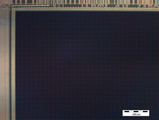
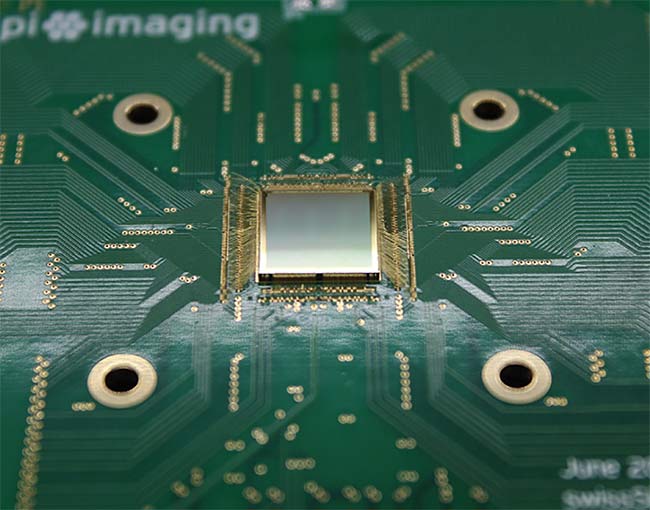
Photonics magazine has a new article about Pi Imaging Technology's high resolution SPAD sensor array; some excerpts below.


As the performance capabilities and sophistication of these detectors have expanded, so too have their value and impact in applications ranging from astronomy to the life sciences.

As their name implies, single-photon avalanche diodes (SPADs) detect single particles of light, and they do so with picosecond precision. Single-pixel SPADs have found wide use in astronomy, flow cytometry, fluorescence lifetime imaging microscopy (FLIM), particle sizing, quantum computing, quantum key distribution, and single- molecule detection. Over the last 10 years, however, SPAD technology has evolved through the use of standard complementary metal-oxide-semiconductor (CMOS) technology. This paved the way for arrays and image sensor architectures that could increase the number of SPAD pixels in a compact and scalable way. 

Compared to single-pixel SPADs, arrays offer improved spatial resolution and signal-to-noise ratio (SNR). In confocal microscopy applications, for example, each pixel in an array acts as a virtual small pinhole with good lateral and axial resolution, while multiple pixels collect the signal of a virtual large pinhole.


Challenges: 

Early SPADs produced as single-point detectors in custom processes offered poor scalability. In 2003, researchers started using standard CMOS technology to build SPAD arrays. This change in design and production platform opened up the possibility to reliably produce high-pixel-count SPAD detectors, as well as invent and integrate new pixel circuity for quenching and recharging, time tagging, and photon-counting functions. Data handling in these devices ranged from simple SPAD pulse outputting to full digital signal processing.
Close collaboration between SPAD developers and CMOS fabs, however, has helped SPAD technology overcome many of its sensitivity and noise challenges by adding SPAD-specific layers into the semiconductor process flow, design innovations in SPAD guard rings, and enhanced fill factors made possible by microlenses. 


Applications:

Research on SPADs also focused on the technology’s potential in biomedical applications, such as Raman spectroscopy, FLIM, and positron emission tomography (PET).

FLIM [fluorescence lifetime imaging microscopy] benefits from the use of SPAD arrays, which allow faster imaging speeds by increasing the sustainable count rate via pixel parallelization. SPAD image sensors enhanced with time-gating functions can further expand the implementation of FLIM to nonconfocal microscopic modalities and thus establish FLIM in a broader range of potential applications, such as spatial multiplexed applications in a variety of biological disciplines including genomics, proteomics, and other “-omics” fields.

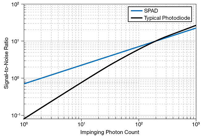
One additional application where SPAD technology is forging performance enhancements is high-speed imaging, in which image sensors typically suffer from low SNR. The shorter integration times in these operations lead to lower photon collection and pixel blur, while the faster readout speeds increase noise in the collected image. SPAD image sensors fully eliminate this noise to offer Poisson-maximized SNR. 


A signal-to-noise ratio (SNR) comparison between a SPAD with 50% sensitivity and a typical photodiode with 80% sensitivity, both with equivalent readout noise of 10 e− (representative only for high-speed readout mode). Courtesy of Pi Imaging Technology.


A demonstration of SNR differences between a typical photodiode with 80% sensitivity and 10 e− signal (representative only for high-speed readout mode) equivalent readout noise (top) and a SPAD with 50% sensitivity (bottom), both at 10 impinging photons average. Courtesy of Pi Imaging Technology.


A SPAD array system implementation for image-scanning microscopy applications.


A fluorescence lifetime imaging microscopy (FLIM) image of mouse embryo tissue recorded with a single-photon-counting confocal microscope. Courtesy of PicoQuant.


About Pi Imaging:

Pi Imaging Technology is fundamentally changing the way we detect light. We do that by creating photon-counting arrays with the highest sensitivity and lowest noise.

We enable our partners to introduce innovative products. The end-users of these products perform cutting-edge science, develop better products and services in life science and quantum information.

Pi Imaging Technology bases its technology on 7 years of dedicated work at TU Delft and EPFL and 6 patent applications. The core of it is a single-photon avalanche diode (SPAD) designed in standard semiconductor technology. This enables our photon-counting arrays to have an unlimited number of pixels and adaptable architectures.


Full article here: https://www.photonics.com/Articles/Single-Photon_Avalanche_Diodes_Sharpen_Spatial/p5/vo211/i1358/a67902

Go to the original article...

Newsight CMOS ToF sensor release

Image Sensors World        Go to the original article...

NESS ZIONA, Israel, Feb. 14, 2022 /PRNewswire/ -- Newsight Imaging - a leading semiconductor innovator developing machine vision sensors, spectral vision chips, and systems - announced today the upcoming release of the NSI9000 one-chip (non-stacked) CMOS image sensor solution for depth imaging. The new chip is equipped with 491,520 depth 5x5 micron pixels (1024x480) (almost 5X more than its closest competitor), global shutter (with up to 132 fps on full resolution), and an estimated depth accuracy of less than 1% of the distance. The sensor is designed for an optimal distance of 0-200 meters. The new chip offers new capabilities at a competitive price to significant growth markets for LiDAR systems, automotive ADAS, Metaverse AR/VR applications, Industry 4.0, and smart city/IOT, including smart traffic 3D vision systems.

The sensor is a result of five years of collaborative innovation by Newsight and its partners such as Fraunhofer and Tower-Jazz. The product offers unique features, including:

Newsight's patented enhanced Time-Of-Flight (eTOF) technology that is well demonstrated on the currently available NSI1000 sensor chip. This technology enables maximal flexibility using multi-sets of configurations, in-pixel accumulation, and a novel depth calculating method that does not require heavy calculations and expensive MCU.
Event aware unique circuit, which was developed as part of the Israeli smart imaging consortium (https://www.smartimagingiia.com/). The solution enables event driven imaging, while a unique circuit attached to each pixel makes it possible to broadcast only lines with pixels that were changed from a previous frame. This feature is specifically designed for smart-city enabled cameras and smart traffic solutions.
Multi-triangulation: a unique solution for industry 4.0 applications and measurement devices of 480 ultra-accurate depth points, down to micron accuracy for close 3D inspection of production rail objects.
Built in fusion, allowing the sensor to extract a full resolution B/W image together with a depth image from the same frame data, and making image and depth fusion trivial for systems developers.
Chip design using a standard CMOS image sensor process, with only two system power source requirements (1.8V, 3.3V), making it a low-power, easy to integrate, and affordable solution for mass markets.


Eyal Yatskan, Newsight CTO and Co-founder, noted: "Newsight has implemented significant, proven, and innovative ideas in this sensor and accelerated the capabilities of the solution to match the high-end requirements of our customers' target applications. Newsight believes that such advanced solutions can be offered at affordable prices for building high volume best ROI depth imaging products."

Newsight will be offering a complete demo system using its eTOF Lidar reference design starting August 2022.

https://www.prnewswire.com/il/news-releases/newsight-imaging-to-release-the-nsi9000-an-affordable-cmos-image-sensor-providing-advanced-features-for-depth-sensing-and-lidar-applications-with-built-in-etof-technology-and-event-detection-capabilities-301481772.html

Go to the original article...

Apple iPhone LiDAR applications

Image Sensors World        Go to the original article...

Polycam makes apps that leverage the new lidar sensor on Apple's latest iPhone and iPad models.

Their website presents a gallery of objects scanned with their app: https://poly.cam/explore


Original press release about Polycam's new app:

Polycam launches a 3D scanning app for the new iPhone 12 Pro models with a LiDAR sensor. The app allows users to rapidly create high quality, color 3D scans that can be used for 3D visualization and more. Because the scans are dimensionally accurate, they can be used to take measurements of virtually anything in the scan at once, rapidly speeding up workflows for many professionals such as architects and 3D designers. What is perhaps most impressive about Polycam is the speed -- scans which would have taken hours to process on a desktop without a LiDAR device can now be processed in seconds directly on an iPhone. 

As Chris Heinrich, the CEO of Polycam, puts it: "I've worked for years on 3D scanning with more conventional hardware, and what you can do on these LiDAR devices is literally 100x faster than what was possible before".

3D capture is a valuable tool for many industries, and Polycam is already seeing enthusiastic usage from architects, archaeologists, movie set designers and more, via an iPad Pro version that launched earlier this year. With the launch of the iPhone version, Heinrich expects to see adoption from many more users across a wider range of verticals. "Just as smartphones dramatically expanded the reach of photo and video", Heinrich says, "we expect these new LiDAR-enabled smartphones to dramatically increase the reach of 3D capture".

While the launch of the iPhone version is an important milestone, "this is just the beginning", says Heinrich. Many new features and improvements are in the pipeline, from enabling users to create even larger scans, improved scanning accuracy of smaller objects and a suite of 3D editing and AI-driven postprocessing tools to supercharge professional workflows that utilize 3D capture. 

Polycam is available to download on the App Store for the iPhone 12 Pro, 12 Pro Max, and the 2020 iPad Pro family. Sample 3D scans can be found on Sketchfab. Polycam was built by a small team of individuals with a passion for 3D capture, and deep experience in computer vision and 3D design.


[I am curious to know what the real-world challenges and limitations are. In particular, how much do the final results rely on lidar data vs. traditional "photogrammetry" that fuses multiple RGB images with minimal supervision from the lidar for, say, absolute scale? If you have an iPhone/iPad and get to try this app out, please share your thoughts in comments below! ---AI]

Go to the original article...

css.php