OmniVision three-layer stacked sensor

Image Sensors World        Go to the original article...

From Businesswire --- "OMNIVISION Announces World’s Smallest Global Shutter Image Sensor for AR/VR/MR and Metaverse".

OmniVision has announced the industry’s first and only three-layer stacked BSI global shutter (GS) image sensor. The OG0TB is the world’s smallest image sensor for eye and face tracking in AR/VR/MR and Metaverse consumer devices, with a package size of just 1.64mm x 1.64mm, it has a 2.2µm pixel in a 1/14.46-inch optical format (OF). The CMOS image sensor features 400×400 resolution and ultra-low power consumption, ideal for some of the smallest and lightest battery-powered wearables, such as eye goggles and glasses. Ultra-low power consumption is critical for these battery-powered devices, which can have 10 or more cameras per system. Their OG0TB BSI GS image sensor consumes less than 7.2mW at 30 frames per second (fps).


SANTA CLARA, Calif.--(BUSINESS WIRE)--OMNIVISION, a leading global developer of semiconductor solutions, including advanced digital imaging, analog, and touch & display technology, today announced the industry’s first and only three-layer stacked BSI global shutter (GS) image sensor. The OG0TB is the world’s smallest image sensor for eye and face tracking in AR/VR/MR and Metaverse consumer devices, with a package size of just 1.64mm x 1.64mm, it has a 2.2µm pixel in a 1/14.46-inch optical format (OF). The CMOS image sensor features 400x400 resolution and ultra-low power consumption, ideal for some of the smallest and lightest battery-powered wearables, such as eye goggles and glasses.

“OMNIVISION is leading the industry by developing the world’s first three-layer stacked global shutter pixel technology and implementing it in the smallest GS image sensor with uncompromising performance,” said David Shin, staff product marketing manager – IoT/Emerging at OMNIVISION. “We pack all of these features and functions into the world’s smallest ‘ready-to-go’ image sensor, which provides design flexibility to put the camera in the most ideal placement on some of the smallest and slimmest wearable devices.” Shin adds, “Ultra-low power consumption is critical for these battery-powered devices, which can have 10 or more cameras per system. Our OG0TB BSI GS image sensor consumes less than 7.2mW at 30 frames per second (fps).”

The worldwide market for AR/VR headsets grew 92.1% year over year in 2021, with shipments reaching 11.2 million units, according to new data from the International Data Corporation (IDC) Worldwide Quarterly AR/VR Headset Tracker1. New entrants as well as broader adoption from the commercial sector will propel the market further as headset shipments are forecast to grow 46.9% year over year in 2022. In fact, IDC expects this market to experience double-digit growth through 2026 as global shipments of AR/VR headsets surpass 50 million units by the end of the forecast, with a 35.1% compounded annual growth rate (CAGR).

OMNIVISION is supporting the growing market for AR/VR headsets by introducing new products such as the OG0TB GS image sensor, which features the company’s most advanced technology:

 It is built on OMNIVISION’s PureCel®Plus-S stacked-die technology.

 It features a three-layer stacked sensor with pixel size at 2.2µm in a 1/14.46-inch OF to achieve 400x400 resolution.

 Nyxel® technology enables the best quantum efficiency (QE) at the 940nm NIR wavelength for sharp, accurate images of moving objects.

 The sensor’s high modulation transfer function (MTF) enables sharper images with greater contrast and more detail, which is especially important for enhancing decision-making processes in machine vision applications.

 The sensor supports a flexible interface, including MIPI with multi-drop, CPHY, SPI, etc.

The OG0TB GS image sensor will be available for sampling in Q3 2022 and in mass production in the 2H 2023.


PS: It is worth noting that Sony made a claim for "world's first 3 layer stacked CIS" back in 2017 after their ISSCC paper titled "A 1/2.3inch 20Mpixel 3-layer stacked CMOS Image Sensor with DRAM" (DOI: 10.1109/ISSCC.2017.7870268). The three layers consisted of photodiodes, DRAM memory, and mixed-signal ISP. But that was a rolling shutter sensor, whereas this one from OmniVision is a global shutter sensor. 

PPS: Readers of blog who know of any journal or conference publication about OmniVision's new design please share them in the comments below! 


Go to the original article...

STMicro and trinamiX collaboration on face authentication

Image Sensors World        Go to the original article...

https://www.yolegroup.com/industry-news/stmicroelectronics-and-trinamix-collaborate-on-behind-oled-face-authentication-solution-to-be-showcased-live-at-ifa-2022/

STMicroelectronics and trinamiX collaborate on behind-OLED face-authentication solution to be showcased live at IFA 2022

  • Companies will demonstrate full facial authentication solution for smartphone integration and for applications behind OLED screens
  • Solution combines high-performance near-infrared global-shutter image sensor from ST and sophisticated trinamiX algorithm
  • Certified for use in mobile payments according to IIFAA, AndroidTM, and FIDO standards


STMicroelectronics, a global semiconductor leader serving customers across the spectrum of electronics applications, and trinamiX, a wholly owned subsidiary of BASF SE and pioneer of new biometric technologies, today announced their collaboration on a reference design for face authentication. The solution performs behind an OLED screen and on the security level required for mobile payments. A demonstration of this system will be first presented live at IFA 2022 in Berlin on September 2-6.

The joint development and reference design for smartphone OEMs is a full system implementation that integrates illumination, a camera module that combines ST’s global-shutter image sensor with enhanced near-infrared (NIR) sensitivity (VD56G3), and trinamiX’s patent-protected algorithms running on the processor. The system offers a contactless, fast, and reliable authentication method for integration into smartphones and other products requiring user authentication. The solution’s strength lies in a unique technology, which uses skin detection to verify a user’s liveness. In addition to verifying the user’s identity, it effectively differentiates between skin and other materials, to recognize fake presentations like photos, hyper-realistic masks, and deepfakes.

"The collaboration with ST provides us with very small, high-performance image sensors at a competitive price point. This is particularly important for our products in the consumer electronics sector," said Stefan Metz, Head of Smartphone Business Asia at trinamiX. “Furthermore, trinamiX Face Authentication can fully operate behind OLED while maintaining the highest security levels. If required, the high NIR sensitivity of ST’s image sensors supports the easy integration of our solution behind display.” According to Metz, smartphone manufacturers are thus offered a powerful, attractive package: “During the development of our smartphone reference design, we focused on particularly compact hardware sizes without compromising the performance.”

"ST’s advanced image sensors use the company’s process technologies that enable class-leading pixel size while offering both high sensitivity and low crosstalk, delivering significant improvements in performance, size, and system integration. The collaboration with trinamiX provides ST with additional opportunities to extend our support to technologies, use cases, and ecosystems addressing the thriving under-display market in Personal Electronics and beyond," said David Maucotel, Head of the Personal Electronics, Industrial and Mass Market Product Business Line at ST’s Imaging Sub-Group.

In 2021, trinamiX Face Authentication was approved for Android integration and certified according to the high biometric security requirements of Android Biometric Class 3, IIFAA Biometric Face Security Test Requirement, and FIDO Level C – the FIDO alliance’s soon-to-be top standard.

A demonstration of the joint system for face authentication will debut at IFA 2022, taking place in Berlin, Germany on September 2-6. Customer presentations as well as appointments during the fair can be requested at info@trinamiX.de.

Go to the original article...

Yole interview with OmniVision’s marketing director

Image Sensors World        Go to the original article...

https://www.yolegroup.com/player-interviews/security-imaging-industry-omnivision-delivers-state-of-the-art-performance-products/

Security has become the largest CMOS image sensor market segment after mobile and computing devices. From 2021 to 2027, according to Yole Intelligence’s latest report, Imaging for Security 2022, revenue is expected to increase from $2.1 billion to $3.6 billion at a 9% Compound Annual Growth Rate (CAGR). 2020 and 2021 were exceptional years for the security CIS segment, and IP security cameras still provide a major growth opportunity. 


Security imaging is sustained by the growing need for security everywhere: in consumer, commercial, and infrastructure monitoring applications, driven by the increasing adoption of home Internet of Things (IoT) solutions, the demand for video analytics in retail and monitored buildings, the need for more touchless access control solutions, the development of public surveillance in cities and for critical infrastructure. The rise of video analytics, edge computing, and the development of AI vision processors enable a wider range of products.


Florian Domengie, Senior Analyst in the Imaging team at Yole Intelligence, had the opportunity to discuss with Devang Patel, Marketing Director of IoT/Emerging Segment at OMNIVISION, about the recent activities of the company and the current trends in the field of security imaging.

Florian Domengie (FD): Please introduce yourself and OMNIVISION to our readers.

Devang Patel (DP): I am OMNIVISION’s Marketing Director and have a long history in the semiconductor industry in various roles. My missions were dedicated to product management/planning, strategic marketing, and partnerships.
OMNIVISION is a global fabless semiconductor organization that develops advanced digital imaging, analog, and touch & display solutions for multiple applications and industries, including mobile phones; security and surveillance; automotive; computing; medical; and emerging applications. Its award-winning innovative technologies enable a smoother human/machine interface in many of today’s commercial devices.

FD: What new products has OMNIVISION released recently? Which applications are you targeting with these new products?
 

DP: From the security side, our company continues to be at the leading edge in providing discreet, energy-efficient power management solutions as well as the best interface protection products on the market. Indeed, thanks to the emergence of the Internet of Things (IoT), surveillance cameras are no longer limited to enterprise applications such as airports, train stations, banks, and office buildings. Instead, they have become an integral part of retail establishments, smart cities, and smart homes for the purpose of gathering and analyzing Big Data.
Here are a few examples of products developed by our experts:
 OMNIVISION’s OS03B10 CMOS image sensor brings high-quality digital images and high-definition (HD) video to security surveillance, IP, and HD analog cameras in a 3-megapixel (MP) 1/2.7-inch optical format (OF). The OS03B10 image sensor features a 2.5 micron (µm) pixel based on OMNIVISION’s OmniPixel®3-HS technology. The high-performance, cost-effective solution uses high-sensitivity frontside illumination (FSI) to detect objects better than the human eye for true-to-life color reproduction in bright and dark conditions.
 OMNIVISION’s OS02H10 is a 2.9µm, 1080p image sensor that provides a high-value option for adding the premium near-infrared (NIR) and ultra-low light performance of its Nyxel® and PureCel®Plus technologies to mainstream surveillance cameras. This sensor also offers multiple high dynamic range (HDR) options for the best quality 1080p still and video captures of fast-moving objects at 60 frames per second (fps). The OS02H10 provides a high-value option for adding premium near-infrared (NIR), ultra-low light, and HDR performance to high-volume, mainstream security systems with AI functionality. It also offers an ultra-low power mode that consumes 97.7% less power than the normal mode to support long battery life.
 OMNIVISION’s OS04C10 is a 2.0µm pixel, 4 MP resolution image sensor for both IoT and home security cameras. When paired with the designer’s selected platform, the OS04C10 can enable a system’s ultra-low power mode for battery-powered cameras with AI functionality. Additionally, it provides a high 2688 x 1520 resolution with a 16:9 aspect ratio while adding the premium NIR and ultra-low light, SNR1 performance of its Nyxel® and PureCel®Plus technologies. This sensor also offers multiple HDR options for the highest quality 4MP still and video captures of fast-moving objects at 60fps. The OS04C10 is built on the PureCel®Plus pixel architecture to achieve a superior low-noise design, providing an SNR1 that is 150% better than OMNIVISION’s prior-generation OV4689 4MP mainstream security sensor.


FD: There has been very significant growth in CMOS imaging products for the security market these last two years. How do you explain this evolution? What benefits do these bring to this market specifically?

DP: There are many factors. We see that the home security market is growing, including DIY battery-powered types of cameras. You can basically install them by yourself. The number of companies getting into this specific product line is growing.
The second factor is infrastructure. Lots of cities worldwide are adding artificial intelligence to their surveillance. For example, looking at intersections, train stations, and airports, we have seen that the city surveillance infrastructure needs growth supported by government initiatives.
The third factor is AI, which is the big thing that brings higher-resolution cameras into this market.
At Yole Intelligence, part of Yole Group, we have noticed increasing opportunities in all the security imaging market segments: consumer, commercial, and infrastructure.

FD: Which types of applications are becoming popular, and what will sustain growth in the security market in the years to come?

DP: I think commercial, and infrastructure are steadier markets, and we expect them to continue to grow. If you look at the CAGR, infrastructure has slowed down a little during the pandemic. On the consumer side, the need for “smart home” has increased. We have seen a CAGR of about 20% for “smart home”, while the traditional consumer commercial security CAGR is about 11%. As a result, we expect both security imaging market segments, commercial and infrastructure, will continue to grow in the coming years.

FD: Have you seen an increasing penetration of 3D sensing into surveillance and security applications?

DP: So far, it has not been huge. We have seen 3D sensing mentioned for some authentication use cases, but it’s mainly applied to indoor access.

FD: As a leading supplier of CMOS image sensors for security imaging, how do you see the competitive landscape and market demand develop? Is there any geographic differentiation between Europe, America, and Asia?

DP: On the overall landscape, we see that the 1080p resolution market is very competitive and is essentially replacing 720p, which used to be the low end. If you look at the product portfolio from OMNIVISION, as well as our competitors, you will see that more and more 1080p cost-sensitive products are being brought into the market.
In terms of geographical differentiation, 1080p seems to be the norm across the globe. Some applications like doorbells and smart home cameras are looking for higher resolution. Some applications like doorbells and smart home cameras are focusing on higher resolution so that they can deploy AI. To better enable AI, Some applications at the very high end would even deploy 4K2K resolutions. When it comes to city or street surveillance, high resolution is needed for counting the number of people or vehicles or for zooming in for detail. However, that market is small compared to 1080p.
While the race for smaller pixels and increased resolution is still ongoing for mobile, it seems less important for security applications where image quality is preferred.

FD: What is the trend in sensor resolution for security applications? What are the most critical performance parameters?

DP: As we mentioned previously, the resolution trend is not as severe in security compared to the smartphone market. The three key buckets we see in security are firstly the 1080p, which is roughly 2MP. Then the next bucket is 4 or 5MP, and at the high end is the 4K2K. From a volume point of view, the 1080p is by far the lion’s share. The 4 and 5MP would be the next, and then 4K2K are very high-end in terms of critical performance.
The key parameter in security is still low light sensitivity: in low light, how good is your camera? So typically, a larger pixel is used in the market. So, in the security market today, the smallest pixel we see is 1.45μm. Slowly, the smaller pixels are being deployed in security, but the majority are still large pixels.
Lower power consumption is critical for numerous applications, particularly battery-powered consumer security cameras.

FD: How can you address this with your products?

DP: To enable longer battery power, we have a unique solution called always-on architecture. Essentially, we provide a total system approach that involves a sensor with our own video processor that enables very low-power system solutions. We are taking our low-power architecture to a new level with a product we will launch later this year.

FD: There is a trend to bring more video analytics and Artificial Intelligence into security camera products. What is OMNIVISION’s view on this?

DP: Video analytics and AI are hot topics in the industry. We expect video analytics and AI technology, which used to be only at the high end a few years ago, to come down to mid-range or entry-level.
One of the key requirements on the sensor side is providing higher resolution so that you can do video analytics and AI functions simultaneously. To address this need, we have a portfolio of 4 and 5MP image sensors, all the way up to 4K2K, for our customers.

FD: Is there any other message you would like to share with our readers and the industry?

DP: In summary, we see 1080p as the dominant resolution for the foreseeable future. A higher resolution is needed for video analytics and AI applications. Always-on is one of the key features demanded for low-power battery cameras.
Low-light pixel performance is still one of the key criteria for security cameras. At OMNIVISION, we have a product line that addresses low light performance that goes from 1080p all the way to 4K2K. We also provide low-power video processors enabling a long-lasting battery solution.

Go to the original article...

CineD tests ARRI ALEXA 35 cinematography sensor

Image Sensors World        Go to the original article...

In June, this blog shared the announcement of ARRI's new cinematography sensor ALEXA 35. 

Last week CineD published a "lab test" of this sensor. CineD is an independent website that reviews latest advances in cinematography technology,

https://www.cined.com/arri-alexa-35-lab-test-rolling-shutter-dynamic-range-and-latitude-plus-video/


Go to the original article...

EETimes Europe article on emergence of consumer and automotive SWIR imaging

Image Sensors World        Go to the original article...

An article in EETimes Europe from August 24, 2022 argues that huge changes are happening in the consumer and automotive SWIR imaging industry. Some excerpts below.

https://www.eetimes.eu/how-smartphones-will-disrupt-the-swir-imaging-industry

How Smartphones Will Disrupt the SWIR Imaging Industry

August 24, 2022 Axel Clouet and Eric Mounier

Sensing SWIR radiation requires imagers based on other materials, making them orders of magnitude more expensive than silicon-based imagers. Therefore, SWIR’s use today is limited to specific applications in defense, industry, or research.

... [A] pull from the consumer market is inspiring unprecedented changes in the SWIR industry, with the emergence of new technologies and the entrance of game-changing players who may enable market and technology disruption.

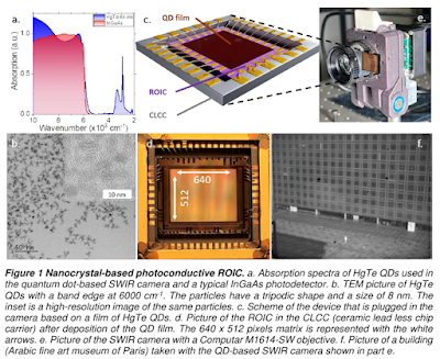
A newer technology, based on quantum dots (QDs), is emerging as a lower-cost alternative to InGaAs. ... with a manufacturing process that is compatible with CMOS, allowing cost reductions by orders of magnitude.

QD technology is still emerging, with the first commercial products released in 2018 for the industry by SWIR Vision Systems.

SWIR’s technology development will be accelerated by the entrance of game-changing players: Sony released its first commercial SWIR imager in 2020, and in 2021, STMicroelectronics announced the development of SWIR imagers based on QDs. ... [both are] leading companies in the consumer and automotive silicon-based imaging industry. Sony introduced a manufacturing method based on copper-to-copper bonding, inherited from its know-how in silicon-based imaging, to make InGaAs SWIR imagers. STMicroelectronics published initial results for its SWIR imagers based on QD technology ... demonstrated high sensitivity, optimized at about 1.4 µm.

[Yole Intelligence] expect[s] the number of industrial cameras to increase significantly in the coming years, thanks to price decreases linked to QD technology penetration and the introduction of new manufacturing processes for InGaAs. These segments could represent a US$828 million market in 2027 at the camera level.

[Since] an artificial SWIR source needs to be used in combination with the imaging system. The SWIR source market should therefore benefit from the growth of the SWIR imaging market. SWIR edge-emitting diode lasers (EELs) are widely used today in the telecommunications market, ... SWIR vertical-cavity surface-emitting lasers (VCSELs) should strongly benefit from the emerging consumer and automotive SWIR markets.


Go to the original article...

Gpixel announces new global shutter GSPRINT 4502 sensor

Image Sensors World        Go to the original article...

Gpixel press release on August 17, 2022:

Gpixel expands high-speed GSPRINT image sensor series with a 2/3” 2.5 MP 3460 fps global shutter GSPRINT4502


Gpixel announces a high-speed global shutter image sensor, GSPRINT4502, a new member of the GSPRINT series taking high speed imaging to another level.


GSPRINT4502 is a 2.5 Megapixel (2048 x 1216), 2/3” (φ10.7 mm), high speed image sensor designed with the latest 4.5 µm charge domain global shutter pixel. It achieves more than 30 ke- charge capacity and less than 4 e- rms read noise, with dynamic range of 68 dB which can be expanded using a multi-slope HDR feature. Utilizing an advanced 65 nm CIS process with light pipe and micro lens technology, the sensor achieves >65% quantum efficiency and < -92 dB parasitic light sensitivity.

GSPRINT4502 can achieve extremely high frame rates up to 3460 fps in 8-bit mode, 1780 fps in 10-bit mode or 850 fps in 12-bit mode, all at full resolution. With 2×2 on-chip charge binning, full well capacity can be further increased to 120 ke- and frame rate to 10,200 fps. GSPRINT4502 supports vertical and horizontal regions of interest for higher frame rates. GSPRINT4502 is perfect for high-speed applications including 3D laser profiling, industrial inspection, high speed video and motion analysis.

Data output from GSPRINT4502 is through 64 pairs sub-LVDS channels running 1.2 Gbps each. Flexible output channel multiplex modes make it possible to reduce frame and data rate to make the sensor compatible with all available camera interface options. GSPRINT4502 is packaged in a 255-pin uPGA ceramic package and will be offered in sealed and removable glass lid versions.

“The market reaction to the GSPRINT high-speed image sensor family provides evidence that a growing number of applications require higher frame rates,” said Wim Wuyts, Chief Commercial Officer of Gpixel. “We are excited to continue to expand the portfolio to bring these high frame rates to more applications.”

GSPRINT4502 engineering samples can be ordered today for delivery in October, 2022. 

About the GSPRINT sensor family

The GSPRINT series is Gpixel’s high-speed global shutter product family, including the 21 MP GSPRINT4521, 10 MP GSPRINT4510 and 2.5 MP GSPRINT4502. The GSPRINT technology will be used to expand the sizes and resolutions available in the family in the future. To learn more about the GSPRINT series, please contact us at: info@gpixel.com
 

About Gpixel

Gpixel provides high-end customized and off-the-shelf CMOS image sensors for industrial, professional, medical, and scientific applications. Gpixel’s standard products include the GMAX and GSPRINT global shutter, fast frame rate sensors, the GSENSE and GLUX high-end scientific CMOS image sensor series, the GL series of line scan imagers, the GLT series of TDI line scan imagers and the GTOF series of iTOF imagers. Gpixel’s broad portfolio of products utilizes the latest technologies to meet the ever-growing demands of the professional imaging market.

Go to the original article...

2023 International Image Sensors Workshop – Call for Papers

Image Sensors World        Go to the original article...

The 2023 International Image Sensors Workshop (IISW) will be held in Scotland from 22-25 May 2023. The first call for papers is now available at this link: 2023 IISW CFP.


FIRST CALL FOR PAPERS

ABSTRACTS DUE DEC 9, 2022
 

2023 International Image Sensor Workshop

Crieff Hydro Hotel, Scotland, UK

22-25 May, 2023


The 2023 International Image Sensor Workshop (IISW) provides a biennial opportunity to present innovative work in the area of solid-state image sensors and share new results with the image sensor community. Now in its 35th year, the workshop will return to an in-person format. The event is intended for image sensor technologists; in order to encourage attendee interaction and a shared experience, attendance is limited, with strong acceptance preference given to workshop presenters. As is the tradition, the 2023 workshop will emphasize an open exchange of information among participants in an informal, secluded setting beside the Scottish town of Crieff. The scope of the workshop includes all aspects of electronic image sensor design and development. In addition to regular oral and poster papers, the workshop will include invited talks and announcement of International Image Sensors Society (IISS) Award winners.

Papers on the following topics are solicited:

Image Sensor Design and Performance
CMOS imagers, CCD imagers, SPAD sensors
New and disruptive architectures
Global shutter image sensors
Low noise readout circuitry, ADC designs
Single photon sensitivity sensors
High frame rate image sensors
High dynamic range sensors
Low voltage and low power imagers
High image quality; Low noise; High sensitivity
Improved color reproduction
Non-standard color patterns with special digital processing
Imaging system-on-a-chip, On-chip image processing

Pixels and Image Sensor Device Physics
New devices and pixel structures
Advanced materials
Ultra miniaturized pixels development, testing, and characterization
New device physics and phenomena
Electron multiplication pixels and imagers
Techniques for increasing QE, well capacity, reducing crosstalk, and improving angular response
Front side illuminated, back side illuminated, and stacked pixels and pixel arrays
Pixel simulation: Optical and electrical simulation, 2D and 3D, CAD for design and simulation, improved models

Application Specific Imagers
Image sensors and pixels for range sensing: LIDAR, TOF,
RGBZ, Structured light, Stereo imaging, etc.
Image sensors with enhanced spectral sensitivity (NIR, UV, IR)
Sensors for DSC, DSLR, mobile, digital video cameras and mirror-less cameras
Array imagers and sensors for multi-aperture imaging,
computational imaging, and machine learning
Sensors for medical applications, microbiology, genome sequencing
High energy photon and particle sensors (X-ray, radiation)
Line arrays, TDI, Very large format imagers
Multi and hyperspectral imagers
Polarization sensitive imagers

Image sensor manufacturing and testing
New manufacturing techniques
Backside thinning
New characterization methods
Defects & leakage current

On-chip optics and imaging process technology
Advanced optical path, Color filters, Microlens, Light guides
Nanotechnologies for Imaging
Wafer level cameras
Packaging and testing: Reliability, Yield, Cost
Stacked imagers, 3D integration
Radiation damage and radiation hard imager


ORGANIZING COMMITTEE

General Workshop Co-Chairs
Robert Henderson – The University of Edinburgh
Guy Meynants – Photolitics and KU Leuven

Technical Program Chair
Neale Dutton – ST Microelectronics

Technical Program Committee
Jan Bogaerts - GPixel, Belgium
Calvin Yi-Ping Chao - TSMC, Taiwan
Edoardo Charbon - EPFL, Switzerland
Bart Dierickx - Caeleste, Belgium
Amos Fenigstein - TowerJazz, Israel
Manylun Ha -  DB Hitek, South Korea
Vladimir Korobov - ON Semiconductor, USA
Bumsuk Kim - Samsung, South Korea
Alex Krymski - Alexima, USA
Jiaju Ma - Gigajot, USA
Pierre Magnan - ISAE, France
Robert Daniel McGrath - Goodix Technology, US 
Preethi Padmanabhan - AMS-Osram, Austria
Francois Roy - STMicroelectronics, France
Andreas Suess - Omnivision Technologies, USA

IISS Board of Directors
Boyd Fowler – OmniVision
Michael Guidash – R.M. Guidash Consulting
Robert Henderson – The University of Edinburgh
Shoji Kawahito – Shizuoka University and Brookman Technology
Vladimir Koifman – Analog Value
Rihito Kuroda – Tohoku University
Guy Meynants – Photolitics
Junichi Nakamura – Brillnics
Yusuke Oike – Sony (Japan)
Johannes Solhusvik – Sony (Norway)
Daniel Van Blerkom – Forza Silicon-Ametek
Yibing Michelle Wang – Samsung Semiconductor

ISS Governance Advisory Committee:
Eric Fossum - Thayer School of Engineering at Dartmouth, USA
Nobukazu Teranishi - University of Hyogo, Japan
Albert Theuwissen - Harvest Imaging, Belgium / Delft University of Technology, The Netherlands

Go to the original article...

Surprises of Single Photon Imaging

Image Sensors World        Go to the original article...

[This is an invited blog post by Prof. Andreas Velten from University of Wisconsin-Madison.]

When we started working on single photon imaging we were anticipating having to do away with many established concepts in computational imaging and photography. Concepts like exposure time, well depth, motion blur, and many others don’t make sense for single photon sensors. Despite this expectation we still encountered several unexpected surprises.

Our first surprise was that SPAD cameras, which typically are touted for low light applications, have an exceptionally large dynamic range and therefore outperform conventional sensors not only in dark, but also in very bright scenes. Due to their hold off time, SPADs reject a growing number of photons at higher flux levels resulting in a nonlinear response curve. The classical light flux is usually estimated by counting photons over a certain time interval. One can instead measure the time between photons or the time a sensor pixel waits for a photon in the active state. This further increases dynamic range so that the saturation flux level is above the safe operating range of the detector pixel and far above eye safety levels. The camera does not saturate. [1][2][3]

The second surprise was that single photon cameras, without further computational improvements, are of limited use in low light imaging situations. In most imaging applications motion of the scene or camera demands short exposure times well below 1 second to avoid motion blur. At light levels low enough to present a challenge to current CMOS sensors results in low photon counts even for a perfect camera. The image looks noisy not because of a problem introduced by the sensor, but because of Poisson noise due to light quantization. The low light capabilities of SPADs only come to bear when long exposure times are used or when motion can be compensated for. Luckily motion compensation strategies inspired by burst photography and event cameras work exceptionally well for SPADs due to the absence of readout noise and inherent motion blur. [4][5][6]

Finally, we assumed early on that single photon sensors have an inherent disadvantage due to larger energy consumption. They either need internal amplification like the SPAD or high frame rates like QIS and qCMOS both of which result in higher power consumption. We learned that the internal amplification process in SPADs makes up a small and decreasing portion of the overall energy consumption of a SPAD. The lions share is spent in transferring and storing the large data volumes resulting from individually processing every single photon. To address the power consumption of SPAD cameras we therefore need to find better ways to compress photon data close to the pixel and be more selective about which photons to process and which to ignore. Even the operation of a conventional CMOS camera can be thought of as a type of compression. Photons are accumulated over an exposure time and only the total is read out after each frame. The challenge for SPAD cameras is to use their access to every single photon and combine it with more sophisticated ways of data compression implemented close to the pixel. [7]

As we transition imaging to widely available high resolution single photon cameras, we are likely in for more surprises. Light is made up of photons. Light detection is a Poisson process. Light and light intensity are derived quantities that are based on ensemble averages over a large number of photons. It is reasonable to assume that detection and processing methods that are based on the classical concept of flux are sub-optimal. The full potential of single photon capture and processing is therefore not yet known. I am hoping for more positive surprises.

References 

[1] Ingle, A., Velten, A., & Gupta, M. (2019). High flux passive imaging with single-photon sensors. In Proceedings of the IEEE/CVF Conference on Computer Vision and Pattern Recognition (pp. 6760-6769). [Project Page]

[2] Ingle, A., Seets, T., Buttafava, M., Gupta, S., Tosi, A., Gupta, M., & Velten, A. (2021). Passive inter-photon imaging. In Proceedings of the IEEE/CVF Conference on Computer Vision and Pattern Recognition (pp. 8585-8595). [Project Page]

[3] Liu, Y., Gutierrez-Barragan, F., Ingle, A., Gupta, M., & Velten, A. (2022). Single-photon camera guided extreme dynamic range imaging. In Proceedings of the IEEE/CVF Winter Conference on Applications of Computer Vision (pp. 1575-1585). [Project Page]

[4] Seets, T., Ingle, A., Laurenzis, M., & Velten, A. (2021). Motion adaptive deblurring with single-photon cameras. In Proceedings of the IEEE/CVF Winter Conference on Applications of Computer Vision (pp. 1945-1954). [Interactive Visualization]

[5] Ma, S., Gupta, S., Ulku, A. C., Bruschini, C., Charbon, E., & Gupta, M. (2020). Quanta burst photography. ACM Transactions on Graphics (TOG), 39(4), 79-1. [Project Page]

[6] Laurenzis, M., Seets, T., Bacher, E., Ingle, A., & Velten, A. (2022). Comparison of super-resolution and noise reduction for passive single-photon imaging. Journal of Electronic Imaging, 31(3), 033042.

[7] Gutierrez-Barragan, F., Ingle, A., Seets, T., Gupta, M., & Velten, A. (2022). Compressive Single-Photon 3D Cameras. In Proceedings of the IEEE/CVF Conference on Computer Vision and Pattern Recognition (pp. 17854-17864). [Project Page]


About the author:

Andreas Velten is Assistant Professor at the Department of Biostatistics and Medical Informatics and the department of Electrical and Computer Engineering at the University of Wisconsin-Madison and directs the Computational Optics Group. He obtained his PhD with Prof. Jean-Claude Diels in Physics at the University of New Mexico in Albuquerque and was a postdoctoral associate of the Camera Culture Group at the MIT Media Lab. He has included in the MIT TR35 list of the world's top innovators under the age of 35 and is a senior member of NAI, OSA, and SPIE as well as a member of Sigma Xi. He is co-Founder of OnLume, a company that develops surgical imaging systems, and Ubicept, a company developing single photon imaging solutions.


Go to the original article...

amsOSRAM announces new sensor Mira220

Image Sensors World        Go to the original article...

  • New Mira220 image sensor’s high quantum efficiency enables operation with low-power emitter and in dim lighting conditions
  • Stacked chip design uses ams OSRAM back side illumination technology to shrink package footprint to just 5.3mm x 5.3mm, giving greater design flexibility to manufacturers of smart glasses and other space-constrained products
  • Low-power operation and ultra-small size make the Mira220 ideal for active stereo vision or structured lighting 3D systems in drones, robots and smart door locks, as well as mobile and wearable devices

Press Release: https://ams-osram.com/news/press-releases/mira220

Premstaetten, Austria (14th July 2022) -- ams OSRAM (SIX: AMS), a global leader in optical solutions, has launched a 2.2Mpixel global shutter visible and near infrared (NIR) image sensor which offers the low-power characteristics and small size required in the latest 2D and 3D sensing systems for virtual reality (VR) headsets, smart glasses, drones and other consumer and industrial applications.

The new Mira220 is the latest product in the Mira family of pipelined high-sensitivity global shutter image sensors. ams OSRAM uses back side illumination (BSI) technology in the Mira220 to implement a stacked chip design, with the sensor layer on top of the digital/readout layer. This allows it to produce the Mira220 in a chip-scale package with a footprint of just 5.3mm x 5.3mm, giving manufacturers greater freedom to optimize the design of space-constrained products such as smart glasses and VR headsets.

The sensor combines excellent optical performance with very low-power operation. The Mira220 offers a high signal-to-noise-ratio as well as high quantum efficiency of up to 38% as per internal tests at the 940nm NIR wavelength used in many 2D or 3D sensing systems. 3D sensing technologies such as structured light or active stereo vision, which require an NIR image sensor, enable functions such as eye and hand tracking, object detection and depth mapping. The Mira220 will support 2D or 3D sensing implementations in augmented reality and virtual reality products, in industrial applications such as drones, robots and automated vehicles, as well as in consumer devices such as smart door locks.

The Mira220’s high quantum efficiency allows device manufacturers to reduce the output power of the NIR illuminators used alongside the image sensor in 2D and 3D sensing systems, reducing total power consumption. The Mira220 features very low power consumption at only 4mW in sleep mode, 40mW in idle mode and at full resolution and 90fps the sensor has a power consumption of 350mW. By providing for low system power consumption, the Mira220 enables wearable and portable device manufacturers to save space by specifying a smaller battery, or to extend run-time between charges.

“Growing demand in emerging markets for VR and augmented reality equipment depends on manufacturers’ ability to make products such as smart glasses smaller, lighter, less obtrusive and more comfortable to wear. This is where the Mira220 brings new value to the market, providing not only a reduction in the size of the sensor itself, but also giving manufacturers the option to shrink the battery, thanks to the sensor’s very low power consumption and high sensitivity at 940nm,” said Brian Lenkowski, strategic marketing director for CMOS image sensors at ams OSRAM.

Superior pixel technology

The Mira220’s advanced back-side illumination (BSI) technology gives the sensor very high sensitivity and quantum efficiency with a pixel size of 2.79μm. Effective resolution is 1600px x 1400px and maximum bit depth is 12 bits. The sensor is supplied in a 1/2.7” optical format.

The sensor supports on-chip operations including external triggering, windowing, and horizontal or vertical mirroring. The MIPI CSI-2 interface allows for easy interfacing with a processor or FPGA. On-chip registers can be accessed via an I2C interface for easy configuration of the sensor.

Digital correlated double sampling (CDS) and row noise correction result in excellent noise performance.

ams OSRAM will continue to innovate and extend the Mira family of solutions, offering customers a choice of resolution and size options to fit various application requirements.

The Mira220 NIR image sensor is available for sampling. More information about Mira220.


Mira220 image sensor achieves high quantum efficiency at 940nm to allow for lower power illumination in 2D and 3D sensing systems
Image: ams

The miniature Mira220 gives extra design flexibility in space-constrained applications such as smart glasses and VR headsets
Image: OSRAM


Go to the original article...

Gigajot article in Nature Scientific Reports

Image Sensors World        Go to the original article...

Jiaju Ma et al. of Gigajot Technology, Inc. have published a new article titled "Ultra‑high‑resolution quanta image sensor with reliable photon‑number‑resolving and high dynamic range capabilities" in Nature Scientific Reports.

Abstract:

Superior low‑light and high dynamic range (HDR) imaging performance with ultra‑high pixel resolution are widely sought after in the imaging world. The quanta image sensor (QIS) concept was proposed in 2005 as the next paradigm in solid‑state image sensors after charge coupled devices (CCD)and complementary metal oxide semiconductor (CMOS) active pixel sensors. This next‑generation image sensor would contain hundreds of millions to billions of small pixels with photon‑number‑resolving and HDR capabilities, providing superior imaging performance over CCD and conventional CMOS sensors. In this article, we present a 163 megapixel QIS that enables both reliable photon‑number‑resolving and high dynamic range imaging in a single device. This is the highest pixel resolution ever reported among low‑noise image sensors with photon‑number‑resolving capability. This QIS was fabricated with a standard, state‑of‑the‑art CMOS process with 2‑layer wafer stacking and backside illumination. Reliable photon‑number‑resolving is demonstrated with an average read noise of 0.35 e‑ rms at room temperature operation, enabling industry leading low‑light imaging performance. Additionally, a dynamic range of 95 dB is realized due to the extremely low noise floor and an extended full‑well capacity of 20k e‑. The design, operating principles, experimental results, and imaging performance of this QIS device are discussed.


Ma, J., Zhang, D., Robledo, D. et al. Ultra-high-resolution quanta image sensor with reliable photon-number-resolving and high dynamic range capabilities. Sci Rep 12, 13869 (2022).

This is an open access article: https://www.nature.com/articles/s41598-022-17952-z.epdf

Go to the original article...

New understanding of color perception theory

Image Sensors World        Go to the original article...

From phys.org a news article about a recent paper that casts doubt on the traditional understanding of how human color perception works: "Math error: A new study overturns 100-year-old understanding of color perception":

A new study corrects an important error in the 3D mathematical space developed by the Nobel Prize-winning physicist Erwin Schrödinger and others, and used by scientists and industry for more than 100 years to describe how your eye distinguishes one color from another. The research has the potential to boost scientific data visualizations, improve TVs and recalibrate the textile and paint industries.

The full paper appears in the Proceedings of the National Academy of Sciences vol. 119 no. 18 (2022). It is titled "The non-Riemannian nature of perceptual color space" authored by Dr. Roxana Bujack and colleagues at Los Alamos National Lab.

The scientific community generally agrees on the theory, introduced by Riemann and furthered by Helmholtz and Schrödinger, that perceived color space is not Euclidean but rather, a three-dimensional Riemannian space. We show that the principle of diminishing returns applies to human color perception. This means that large color differences cannot be derived by adding a series of small steps, and therefore, perceptual color space cannot be described by a Riemannian geometry. This finding is inconsistent with the current approaches to modeling perceptual color space. Therefore, the assumed shape of color space requires a paradigm shift. Consequences of this apply to color metrics that are currently used in image and video processing, color mapping, and the paint and textile industries. These metrics are valid only for small differences. Rethinking them outside of a Riemannian setting could provide a path to extending them to large differences. This finding further hints at the existence of a second-order Weber–Fechner law describing perceived differences.


The key observation that this paper rests on is the concept of "diminishing returns". Statistical analysis of experimental data collected in this paper suggests that the perceived difference between pairs of colors A, B and C that lie along a single shortest path (geodesic) do not satisfy the additive equality.

A commentary by Dr. David Brainard (U. Penn.) about this paper was published in PNAS and is available here: https://color2.psych.upenn.edu/brainard/papers/2022-BrainardPNASCommentary.pdf

Some of the caveats noted in this commentary piece:

First, the authors make a first principles assumption that the achromatic locus is a geodesic and use this in their choice of stimuli. This assumption is intuitively appealing in that it would be surprising that the shortest path in color space between two achromatic stimuli would involve a detour through a chromatic stimulus and back. However, the achromatic locus as a geodesic was not empirically established, and more work could be considered to shore up this aspect of the argument. Second, the data were collected using online methods and combined across subjects prior to the analysis. This raises the question of whether the aggregate performance analyzed could be non-Riemannian even when the performance of each individual subject was itself Riemannian. Although it is not immediately obvious whether this could occur, it might be further considered as a possibility.

Phys.org press release: https://phys.org/news/2022-08-math-error-overturns-year-old-perception.html

LANL press release: https://discover.lanl.gov/news/0810-color-perception

PNAS paper: https://www.pnas.org/doi/10.1073/pnas.2119753119

Go to the original article...

Direct ToF Single-Photon Imaging (IEEE TED June 2022)

Image Sensors World        Go to the original article...

The June 2022 issue of IEEE Trans. Electron. Devices has an invited paper titled Direct Time-of-Flight Single-Photon Imaging by Istvan Gyongy et al. from University of Edinburgh and STMicroelectronics. 

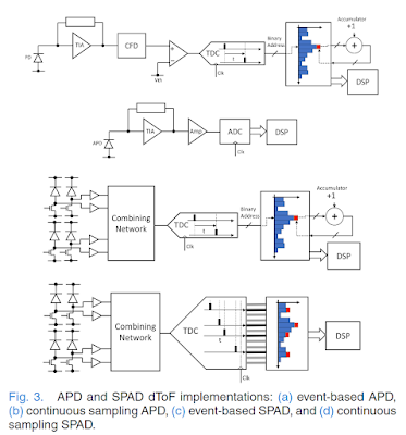
This is a comprehensive tutorial-style article on single-photon 3D imaging which includes a description of the image formation model starting from first principles and practical system design considerations such as photon budget and power requirements.

Abstract: This article provides a tutorial introduction to the direct Time-of-Flight (dToF) signal chain and typical artifacts introduced due to detector and processing electronic limitations. We outline the memory requirements of embedded histograms related to desired precision and detectability, which are often the limiting factor in the array resolution. A survey of integrated CMOS dToF arrays is provided highlighting future prospects to further scaling through process optimization or smart embedded processing.


Go to the original article...

CFP: International Workshop on Image Sensors and Imaging Systems 2022

Image Sensors World        Go to the original article...

The 5th International Workshop on Image Sensors and Imaging Systems (IWISS2022) will be held in December 2022 in Japan. This workshop is co-sponsored by IISS.


-Frontiers in image sensors based on conceptual breakthroughs inspired by applications-

Date: December 12 (Mon) and 13 (Tue), 2022

Venue: Sanaru Hall, Hamamatsu Campus, Shizuoka University 

Access: see https://www.eng.shizuoka.ac.jp/en_other/access/

Address: 3-5-1 Johoku, Nakaku, Hamamatsu, 432-8561 JAPAN

Official language: English


Overview

In this workshop, people from various research fields, such as image sensing, imaging systems, optics, photonics, computer vision, and computational photography/imaging, come together to discuss the future and frontiers of image sensor technologies in order to explore the continuous progress and diversity in image sensors engineering and state-of-the-art and emerging imaging systems technologies. The workshop is composed of invited talks and a poster session. We are accepting approximately 20 poster papers, whose submission starts in August, with deadline on October 14 (Fri), 2022. A Poster Presentation Award will be given to the selected excellent paper. We encourage everyone to submit the latest original work. Every participant is required to register online by December 5 (Mon), 2022. On-site registration is NOT accepted. Since the workshop is operated by a limited number of volunteers, we can offer only minimal service; therefore, no invitation letters for visa applications to enter Japan can be issued.

Latest Information: Call for Paper, Advance Program
http://www.i-photonics.jp/meetings.html#20221212IWISS

Poster Session
Submit a paper: https://www.ite.or.jp/ken/form/index.php?tgs_regid=faf9bc5bde5e430962d98b110ccac65c5ddc6ca5718edb7c80089461c48b9cfa&tgid=ITE-IST&lang=eng&now=20220719133618
Submission deadline: Oct. 14(Fri), 2022 (Only title, authors, and short abstract are required)
Please use the above English page. DO NOT follow the Japanese instructions at the bottom of the page.
Notification of acceptance: by Oct. 21 (Fri)

Manuscript submission deadline: Nov. 21 (Mon), 2022 (2-page English proceeding is required)
One excellent poster will be awarded.

Plenary and Invited Speakers

[Plenary] 

“Deep sensing - Jointly optimize imaging and processing –“ by
Hajime Nagahara (Osaka University, Japan)


[Invited Talks]
- Image Sensors
“InGaAs/InP and Ge-on-Si SPADs for SWIR applications” by Alberto Tosi (Politecnico di Milano, Italy)
“CMOS SPAD-Based LiDAR Sensors with Zoom Histogramming TDC Architectures” by Seong-Jin Kim et al. (UNIST, Korea)
"TBD" by Min-Sun Keel (Samsung Electronics, Korea)
“Modeling and verification of a photon-counting LiDAR” by Sheng-Di Lin (National Yang Ming Chiao Tung Univ., Taiwan)
- Computational Photography/Imaging and applications “Computational lensless imaging by coded optics” by Tomoya Nakamura (Osaka Univ., Japan)
“TBD” by Miguel H. Conde (Siegen Univ.) “TBD” by TBD (Toronto Univ.)
 

- Optics and Photonics
“Optical system integrated time-of-flight and optical coherence tomography for high-dynamic range distance measurement” by Yoshio Hayasaki et al. (Utsunomiya Univ., Japan)
“High-speed/ultrafast holographic imaging using an image sensor” by Yasuhiro Awatsuji et al. (Kyoto Institute of Technology, Japan)
“Near-infrared sensitivity improvement by plasmonic diffraction technology” by Nobukazu Teranishi et al. (Shizuoka Univ, Japan)


Scope
- Image sensor technologies: fabrication process, circuitry, architectures
- Imaging systems and image sensor applications
- Optics and photonics: nanophotonics, plasmonics, microscopy, spectroscopy
- Computational photography/ imaging
- Applications and related topics on image sensors and imaging systems: e.g., multi-spectral imaging, ultrafast imaging, biomedical imaging, IoT, VR/AR, deep learning, ...

Online Registration for Audience
Registration is necessary due to the limited number of available seats.
Registration deadline is Dec. 5 (Mon).
Register and pay online from the following website: <to appear>

Registration Fee
Regular and student: approximately 2,000-yen (~15 USD)
Note: This price is for purchasing the online proceeding of IWISS2022 through the ITE. If you cannot join the workshop due to any reason, no refund will be provided.

Collaboration with MDPI Sensors Special Issue
Special Issue on "Recent Advances in CMOS Image Sensor"
Special issue editor: Dr. De Xing Lioe
Paper submission deadline: Feb. 25 (Sat), 2023
https://www.mdpi.com/journal/sensors/special_issues/CMOS_image_sensor
The poster presenters are encouraged to submit a paper to this special issue!
Note-1: Those who do not give a presentation in the IWISS2022 poster session are also welcome to submit a paper!
Note-2: Sensors is an open access journal, the article processing charges (APC) will be applied to accepted papers.
Note-3: For poster presenters of IWISS2022, please satisfy the following conditions.

The submitted extended papers to the special issue should have more than 50% new data and/or extended content to make it a real and complete journal paper. It will be much better if the Title and Abstract are different with that of conference paper so that they can be differentiated in various databases. Authors are asked to disclose that it is conference paper in their cover letter and include a statement on what has been changed compared to the original conference paper.


Sponsored by Technical Group on Information Sensing Technologies (IST),
the Institute of Image Information and Television Engineers (ITE)
Co-sponsored by International Image Sensor Society (IISS), Group of
Information Photonics (IPG) +CMOS Working Group, the Optical Society of
Japan, and innovative Photonics Evolution Research Center (iPERC)
[General Chair] Keiichiro Kagawa (Shizuoka Univ., Japan)
[Technical Program Committee (alphabetical order)]
Chih-Cheng Hsieh (National Tsing Hua Univ., Taiwan)
Keiichiro Kagawa (Shizuoka Univ., Japan)
Takashi Komuro (Saitama Univ., Japan)
De Xing Lioe (Shizuoka Univ., Japan)
Hajime Nagahara (Osaka Univ., Japan)
Atushi Ono (Shizuoka Univ., Japan)
Min-Woong Seo (Samsung Electronics, Korea)
Hiroyuki Suzuki (Gunma Univ., Japan)
Hisayuki Taruki (Toshiba Electronic Devices & Storage Corporation, Japan)
Franco Zappa (Politecnico di Milano, Italy)

Contact for any question about IWISS2022
E-mail: iwiss2022@idl.rie.shizuoka.ac.jp
(Keiichiro Kagawa, Shizuoka Univ., Japan)

Go to the original article...

Sigma Foveon sensor will be ready in 2022

Image Sensors World        Go to the original article...

From PetaPixel:

Sigma’s CEO Kazuto Yamaki has revealed that the company’s efforts in making a full-frame Foveon sensor are on track to be finished by the end of the year. 


Sigma’s Foveon sensors use a proprietary three-layer structure in which red, green, and blue pixels each have their own full layer. In traditional sensors, the three pixels share a single layer in a mosaic arrangement and the camera “fills in” missing colors by examining neighboring pixels.

Since each pixel of a photo is recorded in three colors, the resulting photo should be sharper with better color accuracy and fewer artifacts.


The release had been delayed on at least two occasions in the past due to technical challenges, once in 2020 and again in 2021. The initial announcement about this sensor was made back in 2018. In February 2022, Yamaki indicated that the company was in stage 2 of testing, and the final third stage will involve mass-production testing.

Go to the original article...

Prophesee interview in EETimes

Image Sensors World        Go to the original article...

EETimes has published an interview with CEO of Prophesee about their event sensor technology. Some excerpts below.

 
Prophesee collaborated with Sony on creating the IMX636 event sensor chip.


Meaning of "neuromorphic"

Most companies doing neuromorphic sensing and computing have a similar vision in mind, but implementations and strategies will be different based on varying product, market, and investment constraints. ...

... there is a fundamental belief that the biological model has superior characteristics compared to the conventional ...

Markets targeted

... the sector closest to commercial adoption of this technology is industrial machine vision. ...

The second key market for the IMX 636 is consumer technologies, ... the event–based camera is used alongside a full–frame camera, detecting motion ... correct any blur.

Prophesee is also working with a customer on automotive driver monitoring solutions... Applications here include eye blinking detection, tracking or face tracking, and micro–expression detection. 

Commercialization strategy

The company recently released a new evaluation kit (EVK4) for the IMX 636. Metavision (simulator) SDK for event–based vision has also recently been open–sourced ...


Future Directions

Prophesee plans to continue development of both hardware and software, alongside new evaluation kits, development kits, and reference designs.

Two future directions... 

further reduction of pixel size (pixel pitch) and overall reduction of the sensor to make it suitable for compact consumer applications such as wearables. 

... facilitating the integration of event–based sensing with conventional SoC platforms.

“The closer you get to the acquisition of the information, the better off you are in terms of efficiency and low latency. You also avoid the need to encode and transmit the data. So this is something that we are pursuing.”

“The ultimate goal of neuromorphic technology is to have both the sensing and processing neuromorphic or event–based, but we are not yet there in terms of maturity of this type of solution,”

Full article here: https://www.eetimes.com/neuromorphic-sensing-coming-soon-to-consumer-products/?

Go to the original article...

3D cameras for metaverse

Image Sensors World        Go to the original article...

Press release from II-VI Inc. announces joint effort with Artilux on a SWIR 3D camera for the "metaverse".

https://ii-vi.com/news/ii-vi-incorporated-and-artilux-demonstrate-a-3d-camera-for-enhanced-user-experience-in-the-metaverse/


PITTSBURGH and HSINCHU, TAIWAN, July 18, 2022 (GLOBE NEWSWIRE) – II‐VI Incorporated (Nasdaq: IIVI), a leader in semiconductor lasers, and Artilux, a leader in germanium silicon (GeSi) photonics and CMOS SWIR sensing technology, today announced a joint demonstration of a next-generation 3D camera with much longer range and higher image resolution to greatly enhance user experience in the metaverse.


Investments in the metaverse infrastructure are accelerating and driving the demand for sensors that enable more realistic and immersive virtual experiences. II-VI and Artilux combined their proprietary technologies in indium phosphide (InP) semiconductor lasers and GeSi sensor arrays, respectively, to demonstrate a miniature 3D camera that operates in the short-wavelength infrared (SWIR), at 1380 nm, resulting in significantly higher performance than existing cameras operating at 940 nm.


“The longer infrared wavelength provides better contrasts and reveals material details that are otherwise not visible with shorter-wavelength illumination, especially in outdoor environments,” said Dr. Julie Sheridan Eng, Sr. Vice President, Optoelectronic Devices & Modules Business Unit, II-VI. “By designing a camera that operates at 1380 nm instead of 940 nm, we can illuminate the scene with greater brightness and still remain well within the margins of eye safety requirements. In addition, the atmosphere absorbs more sunlight at 1380 nm than at 940 nm, which reduces background light interference, greatly improving the signal-to-noise ratio and enabling cameras with longer range and better image resolution.”


“The miniature SWIR 3D camera can be seamlessly integrated into next-generation consumer devices, many of which are under development for augmented-, mixed-, and virtual-reality applications,” said Dr. Neil Na, co-founder and CTO of Artilux. “II‑VI and Artilux demonstrated a key capability that will enable the metaverse to become a popular venue for entertainment, work, and play. The SWIR camera demonstration provides a glimpse of the future of 3D sensing in the metaverse, with displays that can identify, delineate, classify, and render image content, or with avatars that can experience real-time eye contact and facial expressions.” 


II-VI provided the highly integrated SWIR illumination module comprising InP edge-emitting lasers that deliver up to 2 W of output power and optical diffusers, in surface-mount technology (SMT) packages for low-cost and high-quality assembly. Artilux’s camera features a high-bandwidth and high-quantum-efficiency GeSi SWIR sensor array based on a scalable CMOS technology platform. Combined, the products enable a broad range of depth-sensing applications in consumer and automotive markets. 


About II-VI Incorporated
II-VI Incorporated, a global leader in engineered materials and optoelectronic components, is a vertically integrated manufacturing company that develops innovative products for diversified applications in communications, industrial, aerospace & defense, semiconductor capital equipment, life sciences, consumer electronics, and automotive markets. Headquartered in Saxonburg, Pennsylvania, the Company has research and development, manufacturing, sales, service, and distribution facilities worldwide. The Company produces a wide variety of application-specific photonic and electronic materials and components, and deploys them in various forms, including integrated with advanced software to support our customers. For more information, please visit us at www.ii-vi.com.


About Artilux
Artilux, renowned for being the world leader of GeSi photonic technology, has been at the forefront of wide-spectrum 3D sensing and consumer optical connectivity since 2014. Established on fundamental technology breakthroughs, Artilux has been making multidisciplinary innovations covering integrated optics, system architecture to computing algorithm, and emerged as an innovation enabler for smartphones, autonomous driving, augmented reality, and beyond. Our vision is to keep pioneering the frontier of photonic technologies and transform them into enrichment for real life experience. We enlighten the path from information to intelligence. Find out more at www.artiluxtech.com.


Go to the original article...

Review of indirect time-of-flight 3D cameras (IEEE TED June 2022)

Image Sensors World        Go to the original article...

C. Bamji et al. from Microsoft published a paper titled "A Review of Indirect Time-of-Flight Technologies" in IEEE Trans. Electron Devices (June 2022).

Abstract: Indirect time-of-flight (iToF) cameras operate by illuminating a scene with modulated light and inferring depth at each pixel by combining the back-reflected light with different gating signals. This article focuses on amplitude-modulated continuous-wave (AMCW) time-of-flight (ToF), which, because of its robustness and stability properties, is the most common form of iToF. The figures of merit that drive iToF performance are explained and plotted, and system parameters that drive a camera’s final performance are summarized. Different iToF pixel and chip architectures are compared and the basic phasor methods for extracting depth from the pixel output values are explained. The evolution of pixel size is discussed, showing performance improvement over time. Depth pipelines, which play a key role in filtering and enhancing data, have also greatly improved over time with sophisticated denoising methods now available. Key remaining challenges, such as ambient light resilience and multipath invariance, are explained, and state-of-the-art mitigation techniques are referenced. Finally, applications, use cases, and benefits of iToF are listed.


Use of time gates to integrate returning light


iToF camera measurement


Modulation contrast vs. modulation frequency used in iToF cameras


Trend of pixel sizes since 2012

Trend of pixel array sizes since 2012

Trend of near infrared pixel quantum efficiencies since 2010


Multigain column readout


Multipath mitigation

DOI link: 10.1109/TED.2022.3145762

Go to the original article...

Amphibious panoramic bio-inspired camera in Nature Electronics

Image Sensors World        Go to the original article...

M. Lee at al. have published a paper titled "An amphibious artificial vision system with a panoramic visual field" in Nature Electronics. This paper is joint work between researchers in Korea (Institute of Basic Science, Seoul National University, Pusan National University) and USA (UT Austin and MIT).

Abstract: Biological visual systems have inspired the development of various artificial visual systems including those based on human eyes (terrestrial environment), insect eyes (terrestrial environment) and fish eyes (aquatic environment). However, attempts to develop systems for both terrestrial and aquatic environments remain limited, and bioinspired electronic eyes are restricted in their maximum field of view to a hemispherical field of view (around 180°). Here we report the development of an amphibious artificial vision system with a panoramic visual field inspired by the functional and anatomical structure of the compound eyes of a fiddler crab. We integrate a microlens array with a graded refractive index and a flexible comb-shaped silicon photodiode array on a spherical structure. The microlenses have a flat surface and maintain their focal length regardless of changes in the external refractive index between air and water. The comb-shaped image sensor arrays on the spherical substrate exhibit an extremely wide field of view covering almost the entire spherical geometry. We illustrate the capabilities of our system via optical simulations and imaging demonstrations in both air and water.


Full paper text is behind a paywall. I could not find a preprint or author copy. However, the supplementary document and figures are freely accessible.
https://www.nature.com/articles/s41928-022-00789-9

Go to the original article...

Amphibious panoramic bio-inspired camera in Nature Electronics

Image Sensors World        Go to the original article...

M. Lee at al. have published a paper titled "An amphibious artificial vision system with a panoramic visual field" in Nature Electronics. This paper is joint work between researchers in Korea (Institute of Basic Science, Seoul National University, Pusan National University) and USA (UT Austin and MIT).

Abstract: Biological visual systems have inspired the development of various artificial visual systems including those based on human eyes (terrestrial environment), insect eyes (terrestrial environment) and fish eyes (aquatic environment). However, attempts to develop systems for both terrestrial and aquatic environments remain limited, and bioinspired electronic eyes are restricted in their maximum field of view to a hemispherical field of view (around 180°). Here we report the development of an amphibious artificial vision system with a panoramic visual field inspired by the functional and anatomical structure of the compound eyes of a fiddler crab. We integrate a microlens array with a graded refractive index and a flexible comb-shaped silicon photodiode array on a spherical structure. The microlenses have a flat surface and maintain their focal length regardless of changes in the external refractive index between air and water. The comb-shaped image sensor arrays on the spherical substrate exhibit an extremely wide field of view covering almost the entire spherical geometry. We illustrate the capabilities of our system via optical simulations and imaging demonstrations in both air and water.


Full paper text is behind a paywall. I could not find a preprint or author copy. However, the supplementary document and figures are freely accessible.
https://www.nature.com/articles/s41928-022-00789-9

Go to the original article...

IEEE International Conference on Computational Photography 2022 in Pasadena (Aug 1-3)

Image Sensors World        Go to the original article...


[Jul 16, 2022] Update from program chair Prof. Ioannis Gkioulekas: All paper presentations will be live-streamed on the ICCP YouTube channel: https://www.youtube.com/channel/UClptqae8N3up_bdSMzlY7eA

You can watch them for free, no registration required. You can also use the live stream to ask the presenting author questions.

ICCP will take place in person in Caltech (Pasadena, CA) from August 1 to 3, 2022. The final program is now available here: https://iccp2022.iccp-conference.org/program/

There will be an exciting line up of:
  • three keynote speakers, Shree Nayar, Changhuei Yang, Joyce Farrell;
  • ten invited speakers, spanning areas from acousto-optics and optical computing, to space exploration and environment conservation; and 
  • 24 paper and more than 80 poster and demo presentations. 


List of accepted papers with oral presentations:

#16: Learning Spatially Varying Pixel Exposures for Motion Deblurring
Cindy Nguyen (Stanford University); Julien N. P. Martel (Stanford University); Gordon Wetzstein (Stanford University)

#43: MantissaCam: Learning Snapshot High-dynamic-range Imaging with Perceptually-based In-pixel Irradiance Encoding
Haley M So (Stanford University); Julien N. P. Martel (Stanford University); Piotr Dudek (School of Electrical and Electronic Engineering, The University of Manchester, UK); Gordon Wetzstein (Stanford University)

#47: Rethinking Learning-based Demosaicing, Denoising, and Super-Resolution Pipeline
Guocheng Qian (KAUST); Yuanhao Wang (KAUST); Jinjin Gu (The University of Sydney); Chao Dong (SIAT); Wolfgang Heidrich (KAUST); Bernard Ghanem (KAUST); Jimmy Ren (SenseTime Research; Qing Yuan Research Institute, Shanghai Jiao Tong University)

#54: Physics vs. Learned Priors: Rethinking Camera and Algorithm Design for Task-Specific Imaging
Tzofi M Klinghoffer (Massachusetts Institute of Technology); Siddharth Somasundaram (Massachusetts Institute of Technology); Kushagra Tiwary (Massachusetts Institute of Technology); Ramesh Raskar (Massachusetts Institute of Technology)

#6: Analyzing phase masks for wide etendue holographic displays
Sagi Monin (Technion – Israel Institute of Technology); Aswin Sankaranarayanan (Carnegie Mellon University); Anat Levin (Technion)

#7: Wide etendue displays with a logarithmic tilting cascade
Sagi Monin (Technion – Israel Institute of Technology); Aswin Sankaranarayanan (Carnegie Mellon University); Anat Levin (Technion)

#65: Towards Mixed-State Coded Diffraction Imaging
Benjamin Attal (Carnegie Mellon University); Matthew O’Toole (Carnegie Mellon University)

#19: A Two-Level Auto-Encoder for Distributed Stereo Coding
Yuval Harel (Tel Aviv University); Shai Avidan (Tel Aviv University)

#35: First Arrival Differential LiDAR
Tianyi Zhang (Rice University); Akshat Dave (Rice University); Ashok Veeraraghavan (Rice University); Mel J White (Cornell); Shahaboddin Ghajari (Cornell University); Alyosha C Molnar (Cornell University); Ankit Raghuram (Rice University)

#46: PS2F: Polarized Spiral PSF for single-shot 3D sensing
Bhargav Ghanekar (Rice University); Vishwanath Saragadam (Rice University); Dushyant Mehra (Rice University); Anna-Karin Gustavsson (Rice University); Aswin Sankaranarayanan (Carnegie Mellon University); Ashok Veeraraghavan (Rice University)

#56: Double Your Corners, Double Your Fun: The Doorway Camera
William Krska (Boston University); Sheila Seidel (Boston University); Charles Saunders (Boston University); Robinson Czajkowski (University of South Florida); Christopher Yu (Charles Stark Draper Laboratory); John Murray-Bruce (University of South Florida); Vivek K Goyal (Boston University)

#8: Variable Imaging Projection Cloud Scattering Tomography
Roi Ronen (Technion); Schechner Yoav (Technion); Vadim Holodovsky (Technion)

#31: DIY hyperspectral imaging via polarization-induced spectral filters
Katherine Salesin (Dartmouth College); Dario R Seyb (Dartmouth College); Sarah Friday (Dartmouth College); Wojciech Jarosz (Dartmouth College)

#57: Wide-Angle Light Fields
Michael De Zeeuw (Carnegie Mellon University); Aswin Sankaranarayanan (Carnegie Mellon University)

#55: Computational Imaging using Ultrasonically-Sculpted Virtual Lenses
Hossein Baktash (Carnegie Mellon University); Yash Belhe (University of California, San Diego); Matteo Scopelliti (Carnegie Mellon University); Yi Hua (Carnegie Mellon University); Aswin Sankaranarayanan (Carnegie Mellon University); Maysamreza Chamanzar (Carnegie Mellon University)

#38: Dynamic structured illumination microscopy with a neural space-time model
Ruiming Cao (UC Berkeley); Fanglin Linda Liu (UC Berkeley); Li-Hao Yeh (Chan Zuckerberg Biohub); Laura Waller (UC Berkeley)

#39: Tensorial tomographic differential phase-contrast microscopy
Shiqi Xu (Duke University); Xiang Dai (University of California San Diego); Xi Yang (Duke University); Kevin Zhou (Duke University); Kanghyun Kim (Duke University); Vinayak Pathak (Duke University); Carolyn Glass (Duke University); Roarke Horstmeyer (Duke University)

#42: Style Transfer with Bio-realistic Appearance Manipulation for Skin-tone Inclusive rPPG
Yunhao Ba (UCLA); Zhen Wang (UCLA); Doruk Karinca (University of California, Los Angeles); Oyku Deniz Bozkurt (UCLA); Achuta Kadambi (UCLA)#4: Robust Scene Inference under Dual Image Corruptions
Bhavya Goyal (University of Wisconsin-Madison); Jean-Francois Lalonde (Université Laval); Yin Li (University of Wisconsin-Madison); Mohit Gupta (University of Wisconsin-Madison)

#9: Time-of-Day Neural Style Transfer for Architectural Photographs
Yingshu Chen ( The Hong Kong University of Science and Technology); Tuan-Anh Vu (The Hong Kong University of Science and Technology); Ka-Chun Shum (The Hong Kong University of Science and Technology); Binh-Son Hua (VinAI Research); Sai-Kit Yeung (Hong Kong University of Science and Technology)

#25: MPS-NeRF: Generalizable 3D Human Rendering from Multiview Images
Xiangjun Gao (Beijing institute of technology); Jiaolong Yang (Microsoft Research); Jongyoo Kim (Microsoft Research Asia); Sida Peng (Zhejiang University); Zicheng Liu (Microsoft); Xin Tong (Microsoft)

#26: Differentiable Appearance Acquisition from a Flash/No-flash RGB-D Pair
Hyun Jin Ku (KAIST); Hyunho Ha (KAIST); Joo-Ho Lee (Sogang University); Dahyun Kang (KAIST); James Tompkin (Brown University); Min H. Kim (KAIST)

#17: HiddenPose: Non-line-of-sight 3D Human Pose Estimation
Ping Liu (ShanghaiTech University); Yanhua Yu (ShanghaiTech University); Zhengqing Pan (ShanghaiTech University); Xingyue Peng (ShanghaiTech University); Ruiqian Li (ShanghaiTech University); wang yh (ShanghaiTech University ); Shiying Li (ShanghaiTech University); Jingyi Yu (Shanghai Tech University)

#61: Physics to the Rescue: A Physically Inspired Deep Model for Rapid Non-line-of-sight Imaging
Fangzhou Mu (University of Wisconsin-Madison); SICHENG MO (University of Wisconsin-Madison); Jiayong Peng (University of Science and Technology of China); Xiaochun Liu (University of Wisconsin-Madison); Ji Hyun Nam (University of Wisconsin-Madison); Siddeshwar Raghavan (Purdue University); Andreas Velten (University of Wisconsin-Madison); Yin Li (University of Wisconsin-Madison)

Go to the original article...

Detailed depth maps from gated cameras

Image Sensors World        Go to the original article...

Recent work from Princeton University's computational imaging lab shows a new method for generating highly detailed depth maps from a gated camera. 

This work was presented at the recent IEEE/CVF Computer Vision and Pattern Recognition 2022 conference in New Orleans.

Abstract: Gated cameras hold promise as an alternative to scanning LiDAR sensors with high-resolution 3D depth that is robust to back-scatter in fog, snow, and rain. Instead of sequentially scanning a scene and directly recording depth via the photon time-of-flight, as in pulsed LiDAR sensors, gated imagers encode depth in the relative intensity of a handful of gated slices, captured at megapixel resolution. Although existing methods have shown that it is possible to decode high-resolution depth from such measurements, these methods require synchronized and calibrated LiDAR to supervise the gated depth decoder – prohibiting fast adoption across geographies, training on large unpaired datasets, and exploring alternative applications outside of automotive use cases. In this work, propose an entirely self-supervised depth estimation method that uses gated intensity profiles and temporal consistency as a training signal. The proposed model is trained end-to-end from gated video sequences, does not require LiDAR or RGB data, and learns to estimate absolute depth values. We take gated slices as input and disentangle the estimation of the scene albedo, depth, and ambient light, which are then used to learn to reconstruct the input slices through a cyclic loss. We rely on temporal consistency between a given frame and neighboring gated slices to estimate depth in regions with shadows and reflections. We experimentally validate that the proposed approach outperforms existing supervised and self-supervised depth estimation methods based on monocular RGB and stereo images, as well as supervised methods based on gated images. Code is available at https://github.com/princeton-computationalimaging/Gated2Gated.


An example gated imaging system is pictured in the bottom left and consists of a synchronized camera and a not shown VECSL flash illumination source. The system allows to integrate the scene response for narrow depth ranges as illustrated in the bottom row. Therefore, the overlapping gated slices contain implicit depth information according to the time-of-flight principle at image resolution. In comparison the illustrated LiDAR sensors in the top left send out point wise illumination pulses causing a sparse depth representation depicted in the top row. Our proposed self-supervised Gated2Gated learning technique recovers this dense depth information (middle row) from the shown set of three gated images, by learning from temporal and gated illumination cues.

The paper shows results in a variety of challenging driving conditions such as nighttime, fog, rain and snow.

A. Walia et al., "Gated2Gated: Self-Supervised Depth Estimation from Gated Images", CVPR 2022.

Go to the original article...

3D Wafer Stacking: Review paper in IEEE TED June 2022 Issue

Image Sensors World        Go to the original article...

In IEEE Trans. Electr. Dev. June 2022 issue, in a paper titled "A Review of 3-Dimensional Wafer Level Stacked Backside Illuminated CMOS Image Sensor Process Technologies," Wuu et al. write:

Over the past 10 years, 3-dimensional (3-D) wafer-level stacked backside Illuminated (BSI) CMOS image sensors (CISs) have undergone rapid progress in development and performance and are now in mass production. This review paper covers the key processes and technology components of 3-D integrated BSI devices, as well as results from early devices fabricated and tested in 2007 and 2008. This article is divided into three main sections. Section II covers wafer-level bonding technology. Section III covers the key wafer fabrication process modules for BSI 3-D waferlevel stacking. Section IV presents the device results.


This paper has quite a long list of acronyms. Here is a quick reference:
BDTI = backside deep trench isolation
BSI = backside illumination
BEOL = back end of line
HB = hybrid bonding
TSV = through silicon via
HAST = highly accelerated (temperature and humidity) stress test
SOI = silicon on insulator
BOX = buried oxide

Section II goes over wafer level direct bonding methods.


Section III discusses important aspects of stacked design development for BSI (wafer thinning, hybrid bonding, backside deep trench isolation, pyramid structure to improve quantum efficiency, use of high-k dielectric film to deal with crystal defects, and pixel performance analyses).


Section IV shows some results of early stacked designs.


Full article: https://doi.org/10.1109/TED.2022.3152977

Go to the original article...

Xiaomi 12s will have a 1" sensor

Image Sensors World        Go to the original article...

From PetaPixel:

Xiaomi has announced that it’s upcoming 12S Ultra will use the full size of Sony’s IMX989 1-inch sensor. The phone, which is also co-developed with Leica, will be announced on July 4.


Xiaomi’s Lei Jun says that the 1-inch sensor that is coming to the 12S Ultra, crucially, won’t be cropped. How the company plans to deal with physical issues Sony came up against in its phone isn’t clear. Jun also says that Xiaomi didn’t just buy the sensor, but that it was co-developed between the two companies with a total investment cost of $15 million split evenly between them. The fruits of this development will first come to the 12S Ultra before being made available to other smartphone manufacturers, so it’s not exclusive to Xiaomi forever.

... only the 12S Ultra will feature a 1-inch sensor while the 12S and 12S Pro will feature the Sony IMX707 instead.


Go to the original article...

High resolution ToF module from Analog Devices

Image Sensors World        Go to the original article...

Analog Devices has released an industrial-grade megapixel ToF module ADTF3175 and a VGA resolution sensor the ADSD3030 that seeks to bring the highest accuracy ToF technology in the most compact VGA footprint.


The ADTF3175 is a complete Time-of-Flight (ToF) module for high resolution 3D depth sensing and vision systems. Based on the ADSD3100, a 1 Megapixel CMOS indirect Time-of-Flight (iToF) imager, the ADTF3175 also integrates the lens and optical bandpass filter for the imager, an infrared illumination source containing optics, laser diode, laser diode driver and photodetector, a flash memory, and power regulators to generate local supply voltages. The module is fully calibrated at multiple range and resolution modes. To complete the depth sensing system, the raw image data from the ADTF3175 is processed externally by the host system processor or depth ISP.

The ADTF3175 image data output interfaces electrically to the host system over a 4-lane mobile industry processor interface (MIPI), Camera Serial Interface 2 (CSI-2) Tx interface. The module programming and operation are controlled through 4-wire SPI and I2C serial interfaces.

The ADTF3175 has module dimensions of 42mm × 31mm × 15.1mm, and is specified over an operating temperature range of -20°C to 65°C.

Applications:
Machine vision systems
Robotics
Building automation
Augmented reality (AR) systems

Price:
$197 in 1,000 Unit Quantities


The ADSD3030 is a CMOS 3D Time of Flight (ToF)-based 3D depth and 2D visual light imager that is available for integration into 3D sensor systems. The functional blocks required for read out, which include analog-to-digital converters (ADCs), amplifiers, pixel biasing circuitry, and sensor control logic, are built into the chip to enable a cost-effective and simple implementation into systems.

The ADSD3030 interfaces electrically to a host system over a mobile industry processor interface (MIPI), Camera Serial Interface 2 (CSI-2) interface. A lens plus optical band-pass filter for the imager and an infrared light source plus an associated driver are required to complete the working subsystem.

Applications:
Smartphones
Augmented reality (AR) and virtual reality (VR)
Machine vision systems (logistics and inventory)
Robotics (consumer and industrial)


Go to the original article...

Labforge releases new 20.5T ops/s AI machine vision camera

Image Sensors World        Go to the original article...

Labforge has designed and developed a smart camera called Bottlenose which supports 20.5 trillion operations/second processing power and on-board AI, depth, feature points & matching, and a powerful ISP. The target audience is robotics and automation. They have built the camera around a Toshiba Visconti-5 processor. The current models are available as both stereo and monocular versions with IMX577 Sony image sensors. For future models there will be a range of resolutions and shutter options available. 


Go to the original article...

Sony releases new sensors IMX487, IMX661

Image Sensors World        Go to the original article...

IMX487 UV 8.13MP

[Advertised as "new product launch" but this has been around for a while.]

Global shutter CMOS image sensor specialized for the UV spectrum

With the structure specially designed for the properties of the UV wavelengths coupled with Pregius S technology, the image sensor can capture undistorted images of moving objects within a UV range of 200–400 nm and at a high frame rate of 193 fps (operated in the 10-bit mode). This image sensor has a potential to expand the scope of application from the conventional use of UV cameras in the inspection of semiconductors, etc. to areas that require high-speed capability, such as sorting of recycled materials.

Low noise

This image sensor has adopted the component materials dedicated for UV range imaging, and a special structure has been developed for its light receiving area. These make it possible to maintain high UV sensitivity while significantly minimizing noises to produce high quality images.

Smaller pixels

The pixels are miniaturized down to 2.74 um while maintaining high UV sensitivity, realizing a small multi-pixel sensor of the 2/3 type with approximately 8.13 megapixels. It serves well with factory automation, but also for many other purposes, notably for outdoor use for infrastructure inspections, by virtue of its portability and high resolution.


IMX661 127MP

The IM661 is a diagonal 56.73 mm (Type 3.6) CMOS active pixel type solid-state image sensor with a square pixel array and 127 M effective pixels. This chip features a global shutter with variable charge-integration time. This chip operates with analog 3.3 V, digital 1.2 V, and interface 1.8 V quadruple power supply. (Applications: FA cameras)


Go to the original article...

Samsung’s ISOCELL HP3 sensor

Image Sensors World        Go to the original article...

Samsung has published details about its now 200MP sensor 'ISOCELL HP3'.

https://semiconductor.samsung.com/image-sensor/mobile-image-sensor/isocell-hp3/

Press release: https://news.samsung.com/global/samsung-unveils-isocell-image-sensor-with-industrys-smallest-0-56%CE%BCm-pixel


Samsung Electronics, a world leader in advanced semiconductor technology, today introduced the 200MP ISOCELL HP3, the image sensor with the industry’s smallest 0.56-micrometer (μm)-pixels.

“Samsung has continuously led the image sensor market trend through its technology leadership in high resolution sensors with the smallest pixels,” said JoonSeo Yim, Executive Vice President of Sensor Business Team at Samsung Electronics. “With our latest and upgraded 0.56μm 200MP ISOCELL HP3, Samsung will push on to deliver epic resolutions beyond professional levels for smartphone camera users.”

Epic Resolution Beyond Pro Levels

Since its first 108MP image sensor roll-out in 2019, Samsung has been leading the trend of next-generation, ultra-high-resolution camera development. Through the steady launch of new image sensors and advancements in performance, the company is once again forging ahead with the 0.56μm 200MP ISOCELL HP3.

The ISOCELL HP3, with a 12 percent smaller pixel size than the predecessor’s 0.64μm, packs 200 million pixels in a 1/1.4” optical format, which is the diameter of the area that is captured through the camera lens. This means that the ISOCELL HP3 can enable an approximately 20 percent reduction in camera module surface area, allowing smartphone manufacturers to keep their premium devices slim.

The ISOCELL HP3 comes with a Super QPD auto-focusing solution, meaning that all of the sensor’s pixels are equipped with auto-focusing capabilities. In addition, Super QPD uses a single lens over four-adjacent pixels to detect the phase differences in both horizontal and vertical directions. This paves way for a more accurate and quicker auto focusing for smartphone camera users.

The sensor also allows users to take videos in 8K at 30 frames-per-second (fps) or 4K at 120fps, with minimal loss in the field of view when taking 8K videos. Combined with the Super QPD solution, users can take movie-like cinematic footage with their mobile devices.

Ultimate Low Light Experience Through ‘Tetra2pixel’

The ISOCELL HP3 also provides an ultimate low-light experience, with the Tetra2pixel technology that combines four pixels into one to transform the 0.56μm 200MP sensor into a 1.12μm 50MP sensor, or a 12.5MP sensor with 2.24μm-pixels by combining 16 pixels into one. The technology enables the sensor to simulate a large-sized pixel sensor to take brighter and more vibrant shots even in dimmed environments, like in-doors or during nighttime.

To maximize the dynamic range of the mobile image sensor, the ISOCELL HP3 adopts an improved Smart-ISO Pro feature. The technology merges image information made from the two conversion gains of Low and High ISO mode to create HDR images. The upgraded version of the technology comes with a triple ISO mode — Low, Mid and High — that further widens the sensor’s dynamic range. In addition, the improved Smart-ISO Pro enables the sensor to express images in over 4 trillion colors (14-bit color depth), 64 times more colors than the predecessor’s 68 billion (12-bit). Furthermore, by supporting staggered HDR along with Smart-ISO Pro, the ISOCELL HP3 can switch between the two solutions depending on the filming environment to produce high-quality HDR images.

Samples of the Samsung ISOCELL HP3 are currently available, and mass production is set to begin this year.


Effective Resolution 16,320 x 12,288 (200M)

Pixel Size 0.56μm

Optical Format 1/1.4"

Color Filter Super QPD Tetra2pixel, RGB Bayer Pattern

Normal Frame Rate 7.5 fps @ full 200 MP, 27 fps @ 50 MP, and 120 fps @ 12.5 MP

Video Frame Rate 30 fps @ 8K, 120 fps @ 4K, and 480 fps @ FHD

Shutter Type Electronic rolling shutter

ADC Accuracy 10-bits

Supply Voltage 2.2 V for analog, 1.8 V for I/O, and 0.9 V for digital core supply

Operating Temperature -20℃ to +85℃

Interface 4 lanes (2.5Gbps per lane) D-PHY / 3 lanes (4.0Gsps per lane) C-PHY

Chroma Tetra2pixel

Auto Focus RGB Bayer Pattern

HDR Smart-ISO Pro (iDCG), Staggered HDR

Output Formats RAW10/12/14

Analog Gain x128 with High Conversion Gain

Product Status Samples Available 

Go to the original article...

NIT SWIR camera based on HgTe quantum cascade detector

Image Sensors World        Go to the original article...

The Institute of Nano Sciences from CNRS-Sorbonne University is currently researching and producing quantum dot materials of HgTe, sensitive in the extended SWIR wavelength range. Through a partnership with NIT, a first sensor-camera was produced.

This technology is promising to design low-cost and small pixel pitch focal plane array, as well as to expand the spectral range of the SWIR camera up to 2.5 µm.

This collaborative program is funded by the French National Research Agency.

This video  presents the technology of quantum cascade detector (QCD) deposition with response up to 2um on NIT ROIC’s, and sample results images in various conditions.


A related paper titled "Photoconductive focal plane array based on HgTe quantum dots for fast and cost-effective short-wave infrared imaging" is in the June 2022 issue of Nanoscale journal.

Abstract: HgTe nanocrystals, thanks to quantum confinement, present a broadly tunable band gap all over the infrared spectral range. In addition, significant efforts have been dedicated to the design of infrared sensors with an absorbing layer made of nanocrystals. However, most efforts have been focused on single pixel sensors. Nanocrystals offer an appealing alternative to epitaxially grown semiconductors for infrared imaging by reducing the material growth cost and easing the coupling to the readout circuit. Here we propose a strategy to design an infrared focal plane array from a single fabrication step. The focal plane array (FPA) relies on a specifically designed readout circuit enabling in plane electric field application and operation in photoconductive mode. We demonstrate a VGA format focal plane array with a 15 μm pixel pitch presenting an external quantum efficiency of 4-5% (15 % internal quantum efficiency) for a cut-off around 1.8 μm and operation using Peltier cooling only. The FPA is compatible with 200 fps imaging full frame and imaging up to 340 fps is demonstrated by driving a reduced area of the FPA. In the last part of the paper, we discuss the cost of such sensors and show that the latter is only driven by labor costs while we estimate the cost of the NC film to be in the 10-20 € range.


Go to the original article...

Reports argue that mobile phone camera market is slowing

Image Sensors World        Go to the original article...

According to a market report from China "global mobile phone image sensor market is declining, and it is recommended to deploy multi-level product lines, combined with production capacity advantages, to impact market share." [English translation]

In the first quarter of 2022, the global mobile phone image sensor shipments will be approximately 1.13 billion units, a year-on-year decrease of approximately 27.0%.
 
Market demand in Europe and mainland China has suffered multiple blows, and the Latin America market may be able to stand out
 
The upgrade of pixel specifications shows polarization, "main camera up, sub camera down"
 
Leading manufacturers will use production capacity advantages to control supply or change the adversity, and local manufacturers will seek opportunities through differentiation
Suggestion: Improve product functional value, upgrade product structure, and be cautious in large-scale expansion


A recent report by TrendForce forecasts that the relative share of quad-camera module market will not grow much between 2021 and 2022. One explanation might be that there is diminishing returns beyond a certain number of cameras and smartphone companies are focusing on algorithmic enhancements to image/video quality which may give similar results.


TrendForce indicates that mobile phone brands are currently curtailing competition in the hardware specifications of mobile phone camera modules but remain focused on photographic and video performance as promotional features of their mobile phones and will emphasize dynamic photography, night photography and other scenarios to highlight product advantages. This can be achieved not only by strengthening the optical performance of the camera module itself but also through algorithms and software, thereby increasing the enthusiasm of mobile phone brands to invest in self-developed chips.

Go to the original article...

Videos du jour – June 24, 2022

Image Sensors World        Go to the original article...

CASS Talks 2022 - Jose Lipovetzky, CNEA, Argentina - April 8, 2022. Viewing ionizing radiation with CMOS image sensors.


Distributed On-Sensor Compute System for AR/VR Devices: A Semi-Analytical Simulation Framework for Power Estimation (Jorge GOMEZ, Research Scientist, Reality Labs, Meta)


tinyML Applications and Systems Session: Millimeter-Scale Ultra-Low-Power Imaging System for Intelligent Edge Monitoring (Andrea BEJARNO-CARBO, PhD Student, University of Michigan, Ann Arbor MI)


This video briefly introduces the Global Shutter product line of PixArt. It provides insights into the key competitiveness of PixArt's Global Shutter products by comparing their ultra-low-power consumption rates and advanced built-ins with other similar products in the market.


Go to the original article...

css.php