Sony to make self-driving sensors that need 70% less power

Image Sensors World        Go to the original article...

From: https://asia.nikkei.com/Business/Automobiles/Sony-to-make-self-driving-sensors-that-need-70-less-power

Sony is developing its own electric vehicles. (Asia Nikkei)
July 19, 2022


TOKYO -- Sony Group will develop a new self-driving sensor that uses 70% less electricity, helping to reduce autonomous systems' voracious appetite for power and extend the range of electric vehicles.
The sensor, made by Sony Semiconductor Solutions, will be paired with new software to be developed by Sompo Holdings-backed startup Tier IV with the goal of cutting the amount of power used by EV onboard systems by 70%. The companies hope to achieve Level 4 technology, allowing cars to drive themselves under certain conditions, by 2030.


Electric vehicles will make up 59% of new car sales globally in 2035, the Boston Consulting Group predicts. Over 30% of trips 5 km and longer are expected to be made in self-driving cars, which rely on large numbers of sensors and cameras and transmit massive amounts of data.


Existing autonomous systems are said to use as much power as thousands of microwave ovens, hindering improvements in the driving range of EVs. Combined with the drain from air conditioning and other functions, EVs could end up with a range at least 35% smaller than on paper, according to Japan's Ministry of Economy, Trade and Industry. If successful, Sony's new sensors would limit this impact to around 10%.


Sony plans to lower the amount of electricity needed in self-driving systems through edge computing, processing as much data as possible through AI-equipped sensors and software on the vehicles themselves instead of transmitting it to external networks. This approach is expected to shrink communication lags as well, making the vehicles safer. 

[Thanks to the anonymous blog comment for sharing the article text.]


Go to the original article...

InP Market Expanding, Proximity Sensor on iPhone 14, Depth Sensing Issues on iPhone 13

Image Sensors World        Go to the original article...

From Electronics Weekly and Yole:

https://www.electronicsweekly.com/news/business/inp-moving-into-consumer-2022-10/

https://www.yolegroup.com/strategy-insights/apple-and-the-compound-semi-industry-the-story-begins/ 

The InP device market is expanding from traditional datacom and telecom towards the consumer reaching about $5.6 billion by 2027, says Yole Developpement.


Datacom and telecom applications are the traditional markets for InP.Land will continue to grow, but the biggest growth driver – with a 37% CAGR between 2021 and 2027 – will be consumer.
The InP supply chain is fragmented, though it is dominated by two vertically integrated American players: Coherent (formerly II-VI) and Lumentum.


The InP supply chain will need more investment with the rise of the consumer applications.
The migration to higher data rates, lower power consumption within data centres, and the deployment of 5G base stations will drive the development and growth of optical transceiver technology in the coming years.
 

As an indispensable building block for high-speed and long-range optical transceivers, InP laser diodes remain the best choice for telecom & datacom photonic applications.
This growth is driven by high volume adoption of high-data-rate modules, above 400G, by big cloud services and national telecom operators requiring increased fiber-optic network capacity.
 

With that in mind, the InP market, long dominated by datacom and telecom applications, is expected grow from $2.5 billion in 2021 to around $5.6 billion in 2027.
 

Yole Intelligence has developed a dedicated report to provide a clear understanding of the InP-based photonics and RF industries. In its InP 2022 report, the company, part of Yole Group, provides a comprehensive view of the InP markets, divided into photonics and RF sectors. It includes market forecasts, technology trends, and supply chain analysis. This updated report covers the markets from wafer to bare die for photonics applications and from wafer to epiwafer for RF applications by volume and revenue.
 

“There has been a lot of speculation on the penetration of InP in consumer applications,” says Yoke’s Ali Jaffal, “the year 2022 marks the beginning of this adoption. For smartphones, OLED displays are transparent at wavelengths ranging from around 13xx to 15xx nm”.
 

OEMs are interested in removing the camera notch on mobile phone screens and integrating the 3D-sensing modules under OLED displays. In this context, they are considering moving to InP EELs to replace the current GaAs VCSELs . However, such a move is not straightforward from cost and supply perspectives.
 

Yole Intelligence noted the first penetration of InP into wearable earbuds in 2021. Apple was the first OEM to deploy InP SWIR proximity sensors in its AirPods 3 family to help differentiate between skin and other surfaces.
 

This has been extended to the iPhone 14 Pro family. The leading smartphone player has changed the aesthetics of its premium range of smartphones, the iPhone 14 Pro family, reducing the size of the notch at the top of the screen to a pill shape.


To achieve this new front camera arrangement, some other sensors, such as the proximity sensor, had to be placed under the display. Will InP penetration continue in other 3D sensing modules, such as dot projectors and flood illuminators? Or could GaAs technology come back again with a different solution for long-wavelength lasers?
 

The impact of Apple adding such a differentiator to its product significantly affects companies in its supply chain, and vice versa.
 

Traditional GaAs suppliers for Apple’s proximity sensors could switch from GaAs to InP platforms since both materials could share similar front-end processing tools.
 

Yole Intelligence certainly expects to see new players entering the InP business as the consumer market represents high volume potential.
 

In addition, Apple’s move could trigger the penetration of InP into other consumer applications, such as smartwatches and automotive LiDAR with silicon photonics platforms.


In other Apple iPhone related news:

The True Depth camera on the iPhone 13 seems to be oversmoothing at distances over 20cm:


Go to the original article...

CellCap3D: Capacitance Calculations for Image Sensor Cells

Image Sensors World        Go to the original article...

Sequoia's CellCap3D is a software tool specifically designed for the capacitance matrix calculation of image sensor cells. It is fast, accurate and easy to use.


Please contact SEQUOIA Design Systems, Inc. for further details at info@sequoiadesignsystems.com

Go to the original article...

Videos du jour for Nov 14, 2022

Image Sensors World        Go to the original article...

Graphene Flagship (https://graphene-flagship.eu/) spearhead project AUTOVISION is developing a new high-resolution image sensor for autonomous vehicles, which can detect obstacles and road curvature even in extreme and difficult driving conditions.


SPAD and CIS camera fusion for high resolution high dynamic range passive imaging (IEEE/CVF WACV 2022) Authors: Yuhao Liu (University of Wisconsin-Madison)*; Felipe Gutierrez-Barragan (University of Wisconsin-Madison); Atul N Ingle (University of Wisconsin-Madison); Mohit Gupta ("University of Wisconsin-Madison, USA "); Andreas Velten (University of Wisconsin - Madison) Description: Reconstruction of high-resolution extreme dynamic range images from a small number of low dynamic range (LDR) images is crucial for many computer vision applications. Current high dynamic range (HDR) cameras based on CMOS image sensor technology rely on multiexposure bracketing which suffers from motion artifacts and signal-to-noise (SNR) dip artifacts in extreme dynamic range scenes. Recently, single-photon cameras (SPCs) have been shown to achieve orders of magnitude higher dynamic range for passive imaging than conventional CMOS sensors. SPCs are becoming increasingly available commercially, even in some consumer devices. Unfortunately, current SPCs suffer from low spatial resolution. To overcome the limitations of CMOS and SPC sensors, we propose a learning-based CMOS-SPC fusion method to recover high-resolution extreme dynamic range images. We compare the performance of our method against various traditional and state-of-the-art baselines using both synthetic and experimental data. Our method outperforms these baselines, both in terms of visual quality and quantitative metrics.


System Semiconductor Image Sensor Explained | 'All About Semiconductor' by Samsung Electronics


tinyML neuromorphic engineering discussion forum:

Neuromorphic Event-based Vision
Christoph POSCH
CTO
PROPHESEE


New Architecture for Visual AI, Oculi Technology Enables Edge Solutions At The Speed Of Machines With The Efficiency of Biology
Charbel RIZK,
Founder CEO
Oculi Inc.


Roman Genov, University of Toronto
Fast Field-Programmable Coded Image Sensors for Versatile Low-Cost Computational Imaging Presented through the Chalk Talks series of the Institute for Neural Computation (UC San Diego)
08/05/22


Go to the original article...

2023 International Image Sensor Workshop (IISW): Final Call for Papers Available

Image Sensors World        Go to the original article...

The final call for papers for 2023 IISW is now available: https://imagesensors.org/2023-international-image-sensor-workshop/

To submit
an abstract, please go to: https://cmt3.research.microsoft.com/IISW2023

The deadline for abstract submission is 11:59pm, Friday December 9th, 2022 (GMT).

The 2023 International Image Sensor Workshop (IISW) provides a biennial opportunity to present innovative work in the area of solid-state image sensors and share new results with the image sensor community. Now in its 35th year, the workshop will return to an in-person format. The event is intended for image sensor technologists; in order to encourage attendee interaction and a shared experience, attendance is limited, with strong acceptance preference given to workshop presenters. As is the tradition, the 2023 workshop will emphasize an open exchange of information among participants in an informal, secluded setting beside the Scottish town of Crieff.

The scope of the workshop includes all aspects of electronic image sensor design and development. In addition to regular oral and poster papers, the workshop will include invited talks and announcement of International Image Sensors Society award winners.


Go to the original article...

Nature paper on an aberration correcting "meta-image" sensor

Image Sensors World        Go to the original article...

A new paper in Nature titled "An integrated imaging sensor for aberration-corrected 3D photography" by Wu et al. from Tsinghua University presents a new meta-optics based aberration correcting image sensor. They also show several applications such as optical flow and depth imaging in addition to atmospheric aberration correction.

The full paper is open access: https://www.nature.com/articles/s41586-022-05306-8

Abstract: Planar digital image sensors facilitate broad applications in a wide range of areas and the number of pixels has scaled up rapidly in recent years. However, the practical performance of imaging systems is fundamentally limited by spatially nonuniform optical aberrations originating from imperfect lenses or environmental disturbances. Here we propose an integrated scanning light-field imaging sensor, termed a meta-imaging sensor, to achieve high-speed aberration-corrected three-dimensional photography for universal applications without additional hardware modifications. Instead of directly detecting a two-dimensional intensity projection, the meta-imaging sensor captures extra-fine four-dimensional light-field distributions through a vibrating coded microlens array, enabling flexible and precise synthesis of complex-field-modulated images in post-processing. Using the sensor, we achieve high-performance photography up to a gigapixel with a single spherical lens without a data prior, leading to orders-of-magnitude reductions in system capacity and costs for optical imaging. Even in the presence of dynamic atmosphere turbulence, the meta-imaging sensor enables multisite aberration correction across 1,000 arcseconds on an 80-centimetre ground-based telescope without reducing the acquisition speed, paving the way for high-resolution synoptic sky surveys. Moreover, high-density accurate depth maps can be retrieved simultaneously, facilitating diverse applications from autonomous driving to industrial inspections.


Go to the original article...

Yole publishes a market report for X-ray detectors

Image Sensors World        Go to the original article...

https://www.yolegroup.com/product/report/x-ray-imaging/


Market dynamics in digital X-ray imaging have been impacted by the Covid crisis, the current geopolitical context and new environmental policies. The Covid crisis upset demand in medical systems in 2020 and 2021. Healthcare facilities prioritized their budgets to fight Covid, boosting static radiography and computed tomography (CT). Many surgeries, mammographies or dental diagnoses have been delayed, slowing demand in these segments by about a year. The medical business eventually returned to its pre-Covid dynamic and is expected to grow from $1,780M in 2021 to $2,128M in 2027 at the detector level. The security business suffered in 2020 and 2021, with airport shutdowns and borders closing. But now the recovery of air transportation and the tense geopolitical context with the Ukraine-Russia war is driving demand in this segment. Security is expected to go from $50M in 2021 to $57M in 2027. Industry also suffered from a global economic downturn due to Covid. However, car electrification is now a good driver for X-ray inspection, which is used in electronics and battery production lines and storage to detect defects. As a result, the segment will grow from $210M in 2021 to $263M in 2027.


 Key Features

  •  Market data on key X-ray detector technologies including flat panel aSi, aSe, IGZO or CMOS, CT detectors and linear sensors over medical, industry, security, and veterinary markets. Historical data are displayed from 2018 to 2021 before forecasting the market up to 2027
  •  Comprehensive analysis of the market trends in the different market segments
  •  Understanding of how health and political crises affect the X-ray imaging market
  •  Market share for flat panel detectors, in value
  •  Comprehensive description of the supply chain from system integrators to semiconductor fabs. Highlights of the main changes since the last update of the report
  •  Comprehensive description of technologies including roadmap on photon-counting technology. Analysis of the penetration of IGZO in flat panels

What's new

  •  The covid crisis upset demand in 2020/2021. Combined with conflicts and trade wars, it forced many players to build new supply chains
  •  Commercialization of the first photon-counting CT scanner by Siemens Healthineers
  •  The biggest CT scan system makers made acquisitions to ensure internal capacity of manufacturing photon-counting detectors
  •  Car electrification is pulling demand for X-ray inspection in electronics and battery production lines

Product objectives

  •  Provide an overview of the digital X-ray imaging industry with a focus on detector components including the different types technologies
  •  Provide an understanding of the main trends in the different segments of digital X-ray imaging with forecast on the market value and associated shipment volumes
  •  Give supply chain insights describing the different levels of integration and the players composing the ecosystem. Providing data of market share for the different types of X-ray detectors
  •  Offering technology understanding about the main innovations with associated challenges and roadmaps

Go to the original article...

Ouster and Velodyne Merger

Image Sensors World        Go to the original article...

In recent news on consolidation in the LiDAR market, Ouster and Velodyne have announced a merger deal.

Ouster makes "digital" LiDAR sensors based on single photon avalanche diode technology whereas Velodyne is known for their more "traditional" avalanche photodiode based spinning LiDARs.

https://investors.ouster.com/news/news-details/2022/Ouster-and-Velodyne-Announce-Proposed-Merger-of-Equals-to-Accelerate-Lidar-Adoption/default.aspx


SAN FRANCISCO--(BUSINESS WIRE)-- Ouster (NYSE: OUST), a leading provider of high-resolution digital lidar, and Velodyne (NASDAQ: VLDR, VLDRW), a leading global player in lidar sensors and solutions, announced that they have entered into a definitive agreement to merge in an all-stock transaction. The proposed merger is expected to drive significant value creation and result in a strong financial position through robust product offerings, increased operational efficiencies, ​​and a complementary customer base in fast-growing end-markets. Ouster and Velodyne will host a joint webcast on November 7, 2022 at 8:30 AM ET to discuss the planned merger.

Key Strengths of the Combined Company:

  • Operational synergies across engineering, manufacturing, and general administration support an optimized cost-structure
  • Robust product offerings, including verticalized software, to serve a broad set of customers
  • Complementary customer base, partners, and distribution channels, coupled with reduced product costs and an innovative roadmap, to accelerate lidar adoption across fast-growing end markets
  • Extensive intellectual property portfolio with 173 granted and 504 pending patents, backed by over 20 years of combined experience in lidar technology innovation
  • World-class leadership team to be led by Dr. Ted Tewksbury as Executive Chairman of the Board and Angus Pacala as Chief Executive Officer
  • Strong financial position with combined cash balance1 of approximately $355 million as of September 30, 2022
  • Compared to stand-alone cost structures as of September 30, 2022, annualized operating expenditure synergies of at least $75 million expected to be realized within 9 months after transaction-close

 “Ouster’s cutting-edge digital lidar technology, evidenced by strong unit economics and the performance gains of our new products, complemented by Velodyne’s decades of innovation, high-performance hardware and software solutions, and established global customer footprint, positions the combined company to accelerate the adoption of lidar technology across fast-growing markets with a diverse set of customer needs,” said Ouster CEO Angus Pacala. “Together, we will aim to deliver the performance customers demand while achieving price points low enough to promote mass adoption.”
 

“Lidar is a valuable enabling technology for autonomy, with the ability to dramatically improve the efficiency, productivity, safety, and sustainability of a world in motion. We aim to create a vibrant and healthy lidar industry by offering both affordable, high-performance sensors to drive mass adoption across a wide variety of customer applications, and by creating scale to drive profitable and sustainable revenue growth,” said Velodyne CEO Dr. Ted Tewksbury. “The combination of Ouster and Velodyne is expected to unlock enormous synergies, creating a company with the scale and resources to deliver stronger solutions for customers and society, while accelerating time to profitability and enhancing value for shareholders.”


The combined company will offer a robust suite of products to continue to serve a diverse set of end-markets and customers while executing on an innovative product roadmap to meet the future needs of the market. A unified engineering team, compelling product roadmap, and focused customer success team will aim to provide best-in-class support to customers to deliver affordable and more performant sensors. Further, management plans to streamline operating expenditures to build an overall cost structure that is in line with the projected revenue growth of the combined company. ​​Ouster and Velodyne had a combined cash balance of approximately $355 million as of September 30, 2022, and aim to realize annualized cost savings of at least $75 million within 9 months after closing the proposed merger. With an expanded global commercial footprint and distribution network, the combined company expects to deliver increased volumes, reduce product costs, and drive sustainable growth.


Leadership and Governance
The combined company will be led by Angus Pacala, who will serve as Chief Executive Officer, and Dr. Ted Tewksbury, who will serve as Executive Chairman of the Board. The Board will be comprised of eight members, with each company appointing an equal number of members. The full Board and executive team will be announced at a later date.
 

Transaction Details
The merger agreement was signed on November 4, 2022. Under the terms of the agreement, each Velodyne share will be exchanged for 0.8204 shares of Ouster at closing. The transaction will result in existing Velodyne and Ouster shareholders each owning approximately 50% of the combined company, based on current shares outstanding.


The merger transactions are subject to customary closing conditions including shareholder approval by both companies. Both companies will continue to operate their businesses independently until the close of the merger transactions. The merger transactions are expected to be completed in the first half of 2023.


Barclays is serving as financial advisor and Latham & Watkins LLP is serving as legal advisor to Ouster. BofA Securities, Inc. is serving as financial advisor and Skadden, Arps, Slate, Meagher & Flom LLP is serving as legal advisor to Velodyne.


Ouster and Velodyne will each file the full text of the merger agreement with the Securities and Exchange Commission with a Form 8-K within four business days of the date of this release. Investors and security holders of each company are advised to review these filings for the full terms of the proposed combination, as well as any future filings made by the companies, including the Form S-4 Registration Statement to be filed by Ouster and related Joint Proxy Statement/Prospectus included therein. See below under “Additional Information and Where to Find It”.
 

Joint Webcast Information
Ouster and Velodyne will host a joint webcast on November 7, 2022 at 8:30 AM ET to discuss the proposed merger.
Investors and analysts can register for the webcast by visiting the following website: https://event.on24.com/wcc/r/4007460/9C27A5975C89846F7B386331F4D80C90. The webcast will be available as a replay for one year on Ouster’s investor website at https://investors.ouster.com and on Velodyne’s investor website at https://investors.velodynelidar.com.

Go to the original article...

Edge Impulse and ConservationX Labs Camera for Ecology and Conservation

Image Sensors World        Go to the original article...

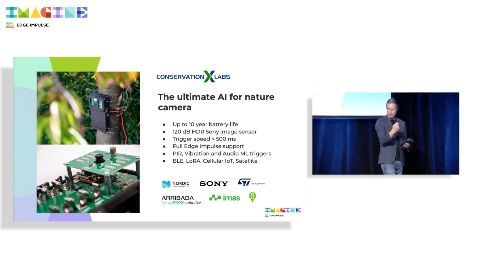
Edge Impulse and Conservation X Labs are teaming up to bring an AI-enabled camera for ecology and wildlife monitoring applications.


https://twitter.com/conservationx/status/1575166560922374144?s=20&t=Nk5lOX69MhcpALGRcMMyHg


Conservation X Labs currently offers a solution called "Sentinel" for AI-on-the-edge using field-deployed cameras and microphones. https://sentinel.conservationxlabs.com/ 

Go to the original article...

Pixelplus automotive CMOS image sensor

Image Sensors World        Go to the original article...

From THEELEC news: https://www.thelec.net/news/articleView.html?idxno=4249

South Korean fabless chip firm Pixelplus will show of engineering samples of its automotive CMOS image sensor to customers during the first quarter.

The new product, called PK5130KA, will begin mass production during the second half of 2023 and contribute to the company’s revenue in 2024, Pixelplus said.

It will the company’s first chip that will be supplied directly to tier-1 suppliers of automobile firms.

Pixelplus had previously supplied such chips through automotive solution firms at a lower price.

Supplying directly to tier-1 suppliers __ called before-market in the industry __ is more difficult due to the harder requirements that they must meet.

Tier-1 suppliers require such chips to meet AEC-Q100 and ISO26262 standards, the global reliability and safety standards.

ISO has ratings from A to D with D being the highest standard. Image sensors require the B grade.

PK5120KA meets these standards, according to Pixelplus. The company is planning to receive the ISO26262 certificate next year.

Pixelplus believes it has a market share of around 5% as of last year in the automotive CMOS image sensor sector.

ONSemiconductor, Sony and Omnivision are the leaders in the market. 

Go to the original article...

Ge-on-Si Image Sensor with NIR Sensitivity

Image Sensors World        Go to the original article...

In a recent preprint (https://arxiv.org/ftp/arxiv/papers/2209/2209.14242.pdf) Ponizovskaya-Devine et al. describe a new Ge-on-Si image sensor with enhanced sensitivity up to 1.7um for NIR applications.


Abstract

We present a Germanium “Ge-on-Si” CMOS image sensor with backside illumination for the near-infrared (NIR) electromagnetic waves (wavelength range 300–1700 nm) detection essential for optical sensor technology. The micro-holes help to enhance the optical efficiency and extend the range to the 1.7 µm wavelength. We demonstrate an optimization for the width and depth of the nano-holes for maximal absorption in the near infrared. We show a reduction in the cross-talk by employing thin SiO2 deep trench isolation in between the pixels. Finally, we show a 26–50% reduction in the device capacitance with the introduction of a hole. Such CMOS-compatible Ge-onSi sensors will enable high-density, ultra-fast and efficient NIR imaging.


Go to the original article...

Ge-on-Si Image Sensor with NIR Sensitivity

Image Sensors World        Go to the original article...

In a recent preprint (https://arxiv.org/ftp/arxiv/papers/2209/2209.14242.pdf) Ponizovskaya-Devine et al. describe a new Ge-on-Si image sensor with enhanced sensitivity up to 1.7um for NIR applications.


Abstract

We present a Germanium “Ge-on-Si” CMOS image sensor with backside illumination for the near-infrared (NIR) electromagnetic waves (wavelength range 300–1700 nm) detection essential for optical sensor technology. The micro-holes help to enhance the optical efficiency and extend the range to the 1.7 µm wavelength. We demonstrate an optimization for the width and depth of the nano-holes for maximal absorption in the near infrared. We show a reduction in the cross-talk by employing thin SiO2 deep trench isolation in between the pixels. Finally, we show a 26–50% reduction in the device capacitance with the introduction of a hole. Such CMOS-compatible Ge-onSi sensors will enable high-density, ultra-fast and efficient NIR imaging.


Go to the original article...

dToF Sensor with In-pixel Processing

Image Sensors World        Go to the original article...

In a recent preprint (https://arxiv.org/pdf/2209.11772.pdf) Gyongy et al. describe a new 64x32 SPAD-based direct time-of-flight sensor with in-pixel histogramming and processing capability.

Abstract
3D flash LIDAR is an alternative to the traditional scanning LIDAR systems, promising precise depth imaging in a compact form factor, and free of moving parts, for applications such as self-driving cars, robotics and augmented reality (AR). Typically implemented using single-photon, direct time-of-flight (dToF) receivers in image sensor format, the operation of the devices can be hindered by the large number of photon events needing to be processed and compressed in outdoor scenarios, limiting frame rates and scalability to larger arrays. We here present a 64 × 32 pixel (256 × 128 SPAD) dToF imager that overcomes these limitations by using pixels with embedded histogramming, which lock onto and track the return signal. This reduces the size of output data frames considerably, enabling maximum frame rates in the 10 kFPS range or 100 kFPS for direct depth readings. The sensor offers selective readout of pixels detecting surfaces, or those sensing motion, leading to reduced power consumption and off-chip processing requirements. We demonstrate the application of the sensor in mid-range LIDAR.


Go to the original article...

TechInsights Webinar on Hybrid Bonding Technologies Nov 15-16

Image Sensors World        Go to the original article...

https://www.techinsights.com/webinar/hybrid-bonding-technology

Hybrid bonding technology is rapidly becoming a standard approach in chipmaking due to its ability to increase connection densities.
This webinar will:
  • Examine different hybrid bonding approaches implemented in recent devices
  • Discuss key players currently using this technology
  • Look to the future of hybrid bonding, discussing potential wins – and pitfalls – to come.
This presentation compiles content from TechInsights’ subject matter experts in Memory, Image Sensor, and Logic, and from Engineers specializing in a variety of reverse engineering techniques. Many of these experts will be on hand for the live Q&A session following the presentation.

 
A preview of the topics that will be discussed:

Advanced Logic

First saw Chip on Wafer (CoW) hybrid bonding technology in the AMD Ryzen 7.
Stacking memory directly with the processor greatly increases available cache memory.
Milestone for system-technology-co-optimization (heterogeneous 3D scaling) described in the International Roadmap for Devices and Systems (IRDS) More Moore roadmap.
 
Image Sensors

We have seen Wafer-to-Wafer (W2W) stacking since 2016 from Sony.
Bond pitches as small as 2.2 µm are common, and the trend points to pitches as small as 1.4 μm.
Direct bond interconnect will ultimately enable digital pixel with in-pixel ADC and stacking of three or more wafers.
 
Memory

Hybrid bonding often used in High Bandwidth Memory (HBM) and 3D Xtacking applications.
Hybrid bonding will be one of most important high density memory enablers.
Further scaling, greater cost effectiveness, fewer defects, and solutions to thermal issues are still required.


Go to the original article...

Samsung announces 200MP ISOCELL HPX

Image Sensors World        Go to the original article...

From: https://r2.community.samsung.com/t5/Galaxy-S/Samsung-announces-200MP-ISCOCELL-HPX-sensor/td-p/12437363

Samsung has announced the ISCOCELL HPX, a new 200MP sensor in China. This follows the June announcement of the ISOCELL HP3 200MP sensor. The ISOCELL HPX has 0.56-micron pixel size, which can reduce the camera module area by 20%, making the smartphone body thinner and smaller.

Furthermore, Samsung employed Advanced DTI (Deep Trench Isolation) technology, which not only separates each pixel individually, but also increases sensitivity to capture crisp and vivid images. Furthermore, the Super QPD autofocus solution enables ISOCELL HPX to have ultra-fast and ultra-precise autofocus.


Tetra-Pixel technology in ISOCELL HPX sensor

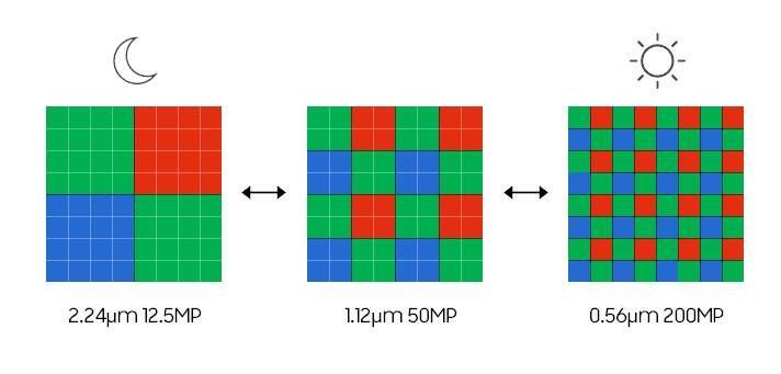
Additionally, the Tetra pixel (16 pixels in one) technology is used in this new sensor that will give positive shooting experience in low light. With the help of this technology, the ISOCELL HPX is able to automatically switch between three different lighting modes depending on the available light: in a well-lit environment, the pixel size is maintained at 0.56 microns (μm), rendering 200 million pixels; in a low-light environment, the pixel is converted to 1.12 microns (μm), rendering 50 million pixels; and in a low-light environment, 16 pixels are combined to create a 2.24 micron (μm) 12.5 million pixel sensor.

According to Samsung, this technology enables ISOCELL HPX to deliver a positive shooting experience in low light and to reproduce sharp, sharp images as much as possible, even when the light source is constrained.

The ISOCELL HPX supports seamless dual HDR shooting in 4K and FHD modes and can capture 8K video at 30 fps. Depending on the shooting environment, Staggered HDR, according to Samsung, captures shadows and bright lights in a scene at three different exposures: low, medium, and high. Then it’ll combine all three exposure photos to produce HDR images and videos of the highest quality.

Additionally, it enables the sensor to render the image at over 4 trillion colours (14-bit colour depth), which is 64 times more than Samsung’s forerunner’s 68 billion colours (12-bit colour depth).

There’s no official wording from the firm regarding the availability. We should know in the coming weeks.

Another source covering this news: https://www.devicespecifications.com/en/news/17401435


Go to the original article...

VISION Stuttgart Videos

Image Sensors World        Go to the original article...

Videos from the recent machine vision trade fair VISION Stuttgart are now available online.

Opening, Camera Technology, Robot Vision, Software & Deep Learning, Optics and Ilumination

3D, Hyperspectral imaging, Vision Processing, Camera Technology, Software & Deep Learning, Standards

Hyperspectral imaging, Camera Technology, Software and Deep Learning, Vision Processing, Optics and Illumination


Go to the original article...

Atomos announces 8K video sensor

Image Sensors World        Go to the original article...

Source: https://announcements.atomos.com/4207684

Atomos completes development of world class 8K video sensor and is exploring commercialisation
[Oct 5, 2022]

Highlights:
Atomos announces that it has completed development of a world class 8K video sensor to allow video cameras to record in 8K ultra high resolution

8K Ultra HD televisions are already in the market from Samsung, Sony and LG but 8K content has been lagging 

The Company is exploring opportunities to commercialise its unique IP and is in discussion with several camera makers

Atomos Limited (‘ASX:AMS’, ‘Atomos’ or the ‘Company’) is pleased to announce that it has completed development of  a  world  class  8K  video  sensor    which  allows  cameras  to  record  in  8K  ultra  high  definition. 

Atomos acquired the intellectual property rights   and technical team from broadcast equipment firm, Grass Valley five years ago to develop a leading-edge 8K video sensor.

8K video has four times the resolution of 4K video and allows video creators much greater flexibility when  zooming in  or  cropping their  shots  during  editing,  as  the  resulting  shot  maintains  sharp resolution. 

There  are  several  8K  televisions  already  in  the  market  from  Samsung,  Sony  and  LG  and  8K  gaming  consoles are expected soon.  8K content however has  been  lagging  because,  outside  of  big  camera  makers such as Sony, owning 8K sensor technology is extremely rare.

Development of Atomos’ 8K sensor is now complete. The Company is actively exploring opportunities for commercialisation and is in discussion with several camera makers who are showing great interest.

Go to the original article...

IC Insights article on CMOS Image Sensors Market

Image Sensors World        Go to the original article...

 https://www.icinsights.com/news/bulletins/CMOS-Image-Sensors-Stall-In-Perfect-Storm-Of-2022/

CMOS Image Sensors Stall in ‘Perfect Storm’ of 2022


For most of the last two decades strong growth in CMOS image sensors pushed this product category to the top of the optoelectronics market, in terms of sales volume, generating over 40% of total opto-semiconductor annual revenues. In 2022, however, the CMOS image sensor market category is on track to suffer its first decline in 13 years with sales expected to fall 7% to $18.6 billion and unit shipments projected to drop 11% to 6.1 billion worldwide, according to IC Insights’ August 3Q Update of The McClean Report service (Figure 1).

The projected 2022 decline in CMOS image sensors comes after two years of meager sales growth in 2020 (+4%) and 2021 (+5%).  This year’s sales drop reflects overall weakness in consumer smartphones and portable computers with digital cameras for video conferencing following an upsurge in demand for Internet connections and online conferencing capabilities during the Covid-19 virus pandemic.  The 3Q Update forecast shows a modest recovery in CMOS image sensors next year with market revenues growing 4% to $19.3 billion and then rising 13% in 2024 to reach a new record high of $21.7 billion.

In addition to weak demand in mainstream consumer camera cellphones and portable computers, CMOS image sensors have been negatively impacted by deteriorating global economic conditions resulting from high inflation and spiking energy costs caused by the Russian war in Ukraine as well as U.S. trade bans on China, recent Covid-19 virus lockdowns in Chinese manufacturing centers, and slowing growth in the number of cameras being packed inside of new smartphones.  Some high-end smartphone models contain five or more cameras, but the average in most handsets has stayed at three (one on the front, facing the user for “selfie” photos and two main cameras on the backside of phones).  IC Insights’ 3Q Update Report says some managers in China have described the image sensor market conditions as a “perfect storm,” combining a slowdown in mainstream mid-range smartphone shipments and an unanticipated pause in the increase of embedded cameras being designed in new handsets.

CMOS image sensor market leader Sony—which accounted for about 43% of CMOS image sensor sales worldwide in 2021—reported a 12.4% sequential decline in image sensor dollar-volume revenues (-2% in Japanese yen) during the company’s fiscal 1Q23 quarter, ended in June 2022.  In the first half of calendar 2022, Sony struggled to match image-resolution requirements for camera phones and its CMOS image sensor sales to leading Chinese system manufacturers were lowered by U.S. trade bans.  Sony still believes excess inventories of phones and image sensors will be reduced by early 2023 and market conditions will “normalize” in the second half of its current fiscal year (ending next March).

Nearly two-thirds of CMOS image sensors are used in cellphones, and that share is expected to fall to about 45% by 2026, according to The McClean Report’s 3Q Update.  A slow–but-steady recovery in CMOS image sensors is forecast to be driven by a new upgrade buying cycle of smartphones and more embedded cameras being added in other systems, especially for automotive automation capabilities, medical applications, and intelligent security networks.  The 3Q Update shows CMOS image sensor sales rising by a CAGR of 6.0% between 2021 and 2026 to reach $26.9 billion in the final year of the forecast.  CMOS image sensor shipments are forecast to grow by a CAGR of 6.9% between 2021 and 2026, reaching 9.6 million units.

Go to the original article...

Videos du jour 2022-09-28: Teledyne, amsOSRAM, IEEE Sensors

Image Sensors World        Go to the original article...


Teledyne e2v's Topaz series of industrial CMOS sensors include 2MP (1920 x 1080) and 1.5MP (1920 x 800) resolution devices. The sensors use state-of-the-art low noise, global-shutter pixel technology to offer powerful solutions and enable compact designs for many applications.


Optimom™ 2M is the first in a range of MIPI CSI-2 optical modules. Powered by Teledyne e2v’s proprietary image sensor technology, Optimom has been thoughtfully designed to ensure there is minimum development effort required for vision-based embedded systems for robotics, logistics, drones, or laboratory equipment. Find out more https://imaging.teledyne-e2v.com/optimom


Time-of-Flight (ToF) sensors from ams enable highly accurate distance measurement and 3D mapping and imaging. Time-of-Flight (ToF) sensors from ams OSRAM are based on proprietary SPAD (Single Photon Avalanche Photodiode) pixel design and time-to-digital converters (TDCs) which have an extremely narrow pulse width. They measure in real time the direct time-of-flight (dToF) of a 940nm VCSEL (laser) emitter’s infrared ray reflected from an object. Accurate distance measurements are used in many applications e.g. presence detection, obstacle avoidance & ranging.


Title: Processing and Chracterisation of an Ultra-Thin Image Sensor Chip in Flexible Foil System
Author: Shuo Wang, Jan Dirk Schulze Spüntrup, Björn Albrecht, Christine Harendt, Joachim Burghartz
Affiliation: Institut für Mikroelektronik Stuttgart IMS CHIPS, Germany

Abstract: Unlike most image sensors, which are planar and inflexible, in this work, an ultra-thin image sensor is performed as a Hybrid System in Foil (HySiF) by using Chip-Film Patch technology, which is a concept for high-performance and ultra-thin flexible electronics. In order to characterize this image sensor embedded in foil, an adapter board for the Andvantest 93000SOIC test system was developed. This paper demonstrates production process of the HySiF and its´ behavior and performance. In addition, the applications and future work of this bendable image sensor in foil system is discussed.


Go to the original article...

ESA-ESTEC Space & Scientific CMOS Image Sensors Workshop 2022

Image Sensors World        Go to the original article...

Registration and other information: https://atpi.eventsair.com/workshop-on-cmos-image-sensors/registration-page/Site/Register

CNES, ESA, AIRBUS DEFENCE & SPACE, THALES ALENIA SPACE, SODERN are pleased to invite you to submit an abstract to the 7th “Space & Scientific CMOS Image Sensors” workshop to be held in ESA-ESTEC on November 22 nd and 23rd 2022 within the framework of the Optics and Optoelectronics COMET (Communities of Experts).

The aim of this workshop is to focus on CMOS image sensors for scientific and space applications.

Although this workshop is organized by actors of the Space Community, it is widely open to other professional imaging applications such as Machine vision, Medical, Advanced Driver Assistance Systems (ADAS), and Broadcast (UHDTV) that boost the development of new pixel and sensor architectures for high end applications.

Furthermore, we would like to invite Laboratories and Research Centres which develop Custom CMOS image sensors with advanced smart design on-chip to join this workshop.

Topics

Abstracts shall preferably address one or more of the following topics:

  • Pixel design (low lag, linearity, FWC, MTF optimization, high quantum efficiency, large pitch pixels)
  • Electrical design (low noise amplifiers, shutter, CDS, high speed architectures, TDI, HDR)
  • On-chip ADC or TDC (in pixel, column, …)
  • On-chip processing (smart sensors, multiple gains, summation, corrections)
  • Electron multiplication, avalanche photodiodes
  • Photon-counting, quanta image sensors
  • Time resolving detectors (gated, time-correlated single-photon counting)
  • Hyperspectral architectures
  • Materials (thin film, optical layers, dopant, high-resistivity, amorphous Si)
  • Processes (backside thinning, hybridization, 3D stacking, anti-reflection coating)
  • Optical design (micro-lenses, trench isolation, filters)
  • Large size devices (stitching, butting)
  • CMOS image sensors with recent space heritage (in-flight performance)
  • High speed interfaces
  • Focal plane architectures

Tutorial Topics

Event-based sensors, SPADs

Industry exhibition

There are a limited number of small stands available for industry exhibitors. If you are interested in exhibiting at the Workshop, please contact the organisers.

Abstract submission

Please send a short abstract on one A4 page maximum in word or pdf format giving the title, the authors name and affiliation, and presenting the subject of your talk, to the organising committee (e-mail addresses are given hereafter).

Workshop format & official language

Oral presentation shall be requested for the workshop. The official language for the workshop is English.

Slide submission

After abstract acceptance notification, the author(s) will be requested to prepare their presentation in pdf or Powerpoint file format, to be presented at the workshop and to provide a copy to the organising committee with an authorization to make it available for all attendees, and on-line for the CCT members.

Calendar

13th September 2022 - Deadline for abstract submission

4th October 2022 - Author notification & preliminary programme

8th November 2022 - Final programme

22nd-23rd November 2022 - Workshop

Organising committee

 Alex MATERNE CNES alex.materne@cnes.fr  +33 5.61.28.15.44
 Nick NELMS ESA nick.nelms@esa.int  +31 71 565 8110
 Kyriaki MINOGLOU ESA kyriaki.minoglou@esa.int  +31 71 565 3797
 Serena RIZZOLO Airbus Defence & Space Serena.rizzolo@airbus.com  +33 5.62.19.62.77
 Stéphane DEMIGUEL Thalès Alenia Space stephane.demiguel@thalesaleniaspace.com  +33 4.92.92.61.89
 Aurelien VRIET SODERN aurelien.vriet@sodern.fr  +33 1.45.95.70.00

Go to the original article...

Calumino raises $10.3m for AI-based thermal sensing

Image Sensors World        Go to the original article...

From Geospatial World: https://www.geospatialworld.net/news/calumino-10-3mn-funding-ai-thermal-sensing-platform/

Calumino, the developer and manufacturer of a proprietary next-generation thermal sensor technology and AI, today announced its $10.3M USD Series A funding. The funding round is led by Celesta Capital and Taronga Ventures, with additional participation from Egis Technology and others. Calumino’s innovation offers the first-ever intelligent sensing platform, which is an aggregator of new and valuable data points on human presence, activity, hazards, and the environment.


As the world’s first thermal sensor to combine A.I. with high performance image sensing, privacy protection, and affordability, Calumino’s platform enables new benefits for a broad range of applications. This includes smart building management, pest control, safety and security, healthcare, and more. The Calumino thermal sensor has been natively designed with a sufficiently low resolution to protect an individual’s privacy, which in turn fills the current market gap between intrusive IP cameras and low performance motion sensors.


Sensing temperatures rather than light, the Calumino thermal sensor maps environments, assets, and individuals and has the ability to detect human presence, activity, and posture. It can also differentiate humans from animals and detect hazardous hotspots, fires, water leaks, and other anomalies. This unique data is essential for saving energy, increasing business operation efficiencies, increasing security and safety, improving life quality, and saving lives.


The Series A funding follows the successful commercialization of Calumino’s technology in the areas of commercial building management and pest control. Most recently, the company has entered the Japanese market with a Mitsubishi Electric subsidiary as a strategic partner, launching its innovative pest control product “Pescle” based upon the Calumino thermal sensor + AI.


“We are incredibly excited about this partnership and plan to roll this product out globally with our partners,” said Marek Steffanson, Founder and CEO of Calumino. “No other technology can differentiate between humans and rodents reliably, in darkness, affordably, intelligently, and with very low data bandwidth – but this application is just the beginning. Our technology is creating an entirely new space in the market and we are incredibly grateful to our investors for their support as we continue to scale production and enable the next generation of intelligent sensing to solve important problems.”


With its Series A proceeds, Calumino plans to expand existing applications and create new use cases. The team also plans to further invest in research and development, as well as expand its global team including new offices in Europe, Taiwan, Japan, and the United States.


“Calumino’s unique technology is helping to drive the proliferation of IoT – the intelligence of things – and enabling for the first time intelligent thermal imaging that is cost-effective, privacy-protecting, and scalable to mass markets,” said Nicholas Brathwaite, Founding Managing Partner of Celesta Capital. “Celesta is excited to offer our financial and intellectual capital support to help Calumino pursue their bold ambitions in becoming the ultimate IoT technology.”


“Calumino’s affordable and intelligent technology is changing the standard of how we live, work and play in real assets. The unique data and insights that Calumino is able to provide will enable asset owners to create safe, secure, and healthy environments using market-leading technology”, said Sven Sylvester, Investment Director at Taronga Ventures.

Go to the original article...

Prophesee closes EUR 50 million Series C

Image Sensors World        Go to the original article...

Prophesee closes €50M C Series round with new investment from Prosperity7 to drive commercialization of revolutionary neuromorphic vision technology;

Becomes EU’s most well-funded fabless semiconductor startup

Link: https://www.prophesee.ai/2022/09/22/prophesee-closes-50million-fundraising-round/

PARIS, September 22, 2022 – Prophesee, the inventor of the world’s most advanced neuromorphic vision systems, today announced the completion of its Series C round of funding with the addition of a new investment from Prosperity7 ventures. The round now totals €50m, including backing from initial Series C investors Sinovation Ventures and Xiaomi. They join an already strong group of international investors from North America, Europe and Japan that includes Intel Capital, Robert Bosch Venture Capital, 360 Capital, iBionext, and the European Investment Bank.

With the investment round, Prophesee becomes EU’s most well-funded fabless semiconductor startup, having raised a total of €127M since its founding in 2014.

Prosperity7 Ventures, the diversified growth global fund of Aramco Ventures – a subsidiary of Saudi Aramco, is on constant search for transformative technologies and innovative business models. Its mission is to invest in the disruptive technologies with the potential to create next-generation technology leaders and bring prosperity on a vast scale. It currently has $1B under management and holds diversified investments across various sectors, including in deep tech and bio-science companies.

 “Gaining the support of such a substantial investor as Prosperity7 adds another globally-focused backer that has a long-term vision and understanding of the requirements to achieve success with a deep tech semiconductor investment. Their support is a testament to the progress achieved and the potential that lies ahead for Prophesee. We appreciate the rigor which they, and all our investors, have used in evaluating our technology and business model and are confident their commitment to a long-term relationship will be mutually beneficial,” said Luca Verre, co-founder and CEO of Prophesee.

The round builds further momentum for Prophesee in accelerating the development and commercialization of its next generation hardware and software products, as well as position it to address new and emerging market opportunities and further scale the company. The support from its investors strengthens its ability to develop business opportunities across key ecosystems in semiconductors, industrial, robotics, IoT and mobile devices.

Event cameras address the challenges of applying computer vision in innovative ways

 “Prophesee is leading the development of a very unique solution that has the potential to revolutionize and transform the way motion is captured and processed.” noted Aysar Tayeb, the Executive Managing Director at Prosperity7. “The company has established itself as a clear leader in applying neuromorphic methods to computer vision with its revolutionary event-based Metavision® sensing and processing approach. With its fundamentally differentiated AI-driven sensor solution, its demonstrated track record with global leaders such as Sony, and its fast-growing ecosystem of more than 5,000 developers using its technology, we believe Prophesee is well-positioned to enable paradigm-shift innovation that brings new levels of safety, efficiency and sustainability to various market segments, including smartphones, automotive, AR/VR and industrial automation.” Aysar further emphasized “Prophesee and its unique team hit the criteria we are constantly searching for in startup companies with truly disruptive, life-changing technologies.”

Prophesee’s approach to enabling machines to see is a fundamental shift from traditional camera methods and aligns directly with the increasing need for more efficient ways to capture and process the dramatic increase in the volume of video input. By utilizing neuromorphic techniques to mimic the way that human brain and eye work, Prophesee’s event-based Metavision technology significantly reduces the amount of data needed to capture information. Among the benefits of the sensor and AI technology are ultra-low latency, robustness to challenging lighting conditions, energy efficiency, and low data rate. This makes it well-suited for a broad range of applications in industrial automation, IoT, consumer electronics that require real-time video data analysis while operating under demanding power consumption, size and lighting requirements.

Prophesee has gained market traction with key partners around the world who are incorporating its technology into sophisticated vision systems for uses cases in smartphones, AR/VR headsets, factory automation and maintenance, science and health research. Its partnership with Sony has resulted in a next generation HD vision sensor that combines Sony’s CMOS image sensor technology with Prophesee’s unique event-based Metavision® sensing technology. It has established commercial partnership with leading machine vision suppliers such as Lucid, Framos, Imago and Century Arks, and its open-source model for accessing its software and development tools has enabled a fast-growing community of 5,000+ developers using the technology in new and innovative ways. 

Go to the original article...

TechInsights on new iPhone 14 camera module

Image Sensors World        Go to the original article...

Full blog article here: https://www.techinsights.com/blog/apple-iphone-14-image-sensor-preliminary-analysis


Go to the original article...

Arducam’s New ToF Camera Module for Embedded Applications

Image Sensors World        Go to the original article...

- Real-time point cloud and depth map.
- Resolution: 240x180@30fps on RPI4/CM4
- Up to 4M measuring distance
- Onboard 940nm laser for both indoor & outdoor uses, no external light source needed.
- V4L2-based video kernel device
- C/C++/Python SDK for userland depth map output and example source code
- ROS ready
- 38 x 38mm board size


Kickstarter link: https://www.kickstarter.com/projects/arducam/time-of-flight-tof-camera-for-raspberry-pi

Go to the original article...

Alpsentek "hybrid" vision sensor for HDR imaging

Image Sensors World        Go to the original article...

From the VISION 2022 exhibition in Stuttgart:

https://www.messe-stuttgart.de/vision/en/visitors/exhibitor-index#/408938/news/news.8e4a0ca4-5e68-418c-9f12-22b682433854

AlpsenTek® launches the ALPIX-Eiger™, a fusion vision sensor for high-end imaging 

AlpsenTek®, a leading developer of fusion vision sensors, announced the launch of the ALPIX-Eiger™ fusion vision sensor chip, specifically designed for high-end imaging applications. Using the original patented Hybrid Vision™ fusion vision technology, ALPIX-Eiger™ enables the fusion of image sensing and event sensing at the pixel level, making the simultaneous output of both image and event streams possible.

ALPIX-Eiger ™ is a patented chip architecture and pixel design with advanced 3D stacking and BSI back-illuminated/backlight technology. With a pixel size of just 1.89µm×1.89µm and a resolution of 8.0 megapixels, it is the smallest pixel size and highest resolution image sensor with event-aware capabilities in the industry. It offers broad application capabilities to small-sized smart devices, such as mobile phones and motion cameras.

High performance

The ALPIX-Eiger™ not only maintains the advantages of image sensors, ensuring full image quality and rich image details but also facilitates event sensing through the patented design of digital-analog mixed signal processing in pixels. This technology allows single pixel to work independently to detect light changes. Having a response speed of microseconds, high frame rate (equivalent to 5000fps), high dynamic range (110dB), low data redundancy and other characteristics helps the image sensor obtain more information and enhances image quality.  Compared with previous event camera solutions, the event stream output by ALPIX-Eiger™ carries color information, which aids color reconstruction of the image and achieves better quality photo and video capabilities.

Wide Applications

In practical applications, intelligent imaging devices equipped with ALPIX-Eiger™ chips can achieve high-end functions such as de-blurring, high frame rate, and super-resolution to facilitate the development of more visual applications. The HDR performance and instantaneous response of the ALPIX-Eiger™ also allow the device to obtain better imaging results at night in scenarios with extreme light and dark contrasts.


Other recent posts about Alpsentek:

https://image-sensors-world.blogspot.com/2022/06/alpsentek-vision-sensor-startup-raises.html

https://image-sensors-world.blogspot.com/2021/11/interview-with-ceo-of-ruisi-zhixin.html

http://image-sensors-world.blogspot.com/2021/10/chinese-startup-ruisizhixin-develops.html

Go to the original article...

ST’s new ToF sensor uses a metalens

Image Sensors World        Go to the original article...

Recent EE Journal article suggests that the 2nd generation time-of-flight proximity sensor from STMicro uses metalenses designed by Metalenz, a Harvard spinoff.

Original article here: https://www.eejournal.com/article/time-of-flight-sensors-trilobites-and-tunable-optics-what-an-unlikely-combo/

Some excerpts below:

Time of Flight Sensors, Trilobites, and Tunable Optics – What an Unlikely Combo!

STMicroelectronics has added a new member to its line of VL53 FlightSense TOF (time of flight) distance/ranging sensors, but this new sensor takes a radical departure from the previous generation by replacing a conventional lensing system with metalenses, developed in conjunction with a startup company called Metalenz and based on technology originally developed in a Harvard University metamaterial lab. According to Metalenz, this is the first commercial product to incorporate its metalens technology.


The resulting TOF sensor can achieve more than double the range – as much as 4m in indoor settings – or it can operate at half the power consumption relative to ST’s previous generation of VL53 TOF sensors. The expanded range and reduced power consumption arise from a combination of a more efficient VCSEL driver circuit and the improved light-gathering ability of the metalens covering the SPAD array. ST’s announcement did not specify a minimum target distance for the VL53L8 sensor, but its predecessor, the VL53L5CX sensor, has a minimum ranging distance of 2cm and an apparent resolution of 1mm, with ±15mm accuracy in the 20-200mm range and 4-11% in the 201-4000mm range, depending on ambient lighting.

Like the earlier VL53L5CX sensor, the new VL53L8 sensor can determine distance to a target or multiple targets simultaneously using either 16 zones at 60Hz or 64 zones at 15Hz, as observed through a 43.5° x 43.5° square field of view. An integrated microcontroller in the TOF sensor delivers range-to-target information directly over an I2C or SPI serial interface and can generate interrupts to wake a host processor when each distance reading is made. Even with all it packs inside, this is a physically tiny sensor, measuring 6.4 x 3.0 x 1.75 mm. It’s supplied as a single, factory-aligned, reflowable component so you can drop it into a variety of products, even small portable ones.


A recent press-release from Metalenz confirms that they have indeed partnered with ST on the new VL53L8 proximity sensor.

Press release: https://www.metalenz.com/the-worlds-first-metasurfaces-have-arrived-on-the-market/

Boston, MA and Geneva, Switzerland – June 9, 2022 – Metalenz, the first company to commercialize meta-optics, and STMicroelectronics (NYSE: STM), a global semiconductor leader serving customers across the spectrum of electronics applications, today announce that ST’s currently released VL53L8 direct Time-of-Flight (dToF) sensor is the highly anticipated market debut of the meta-optics devices developed through their partnership, which was disclosed in June 2021.

Metalenz’s Harvard-born, meta-optics technology can replace existing complex and multi-element lenses and provide additional functionality with a single meta-optic embedded in time-of-flight (ToF) modules from ST, the leading company in supplying 3D sensing modules. The introduction of Metalenz technology in these modules brings performance, power, size, and cost advantages to a multitude of consumer, automotive, and industrial applications. This marks the first time metasurface technology is commercially available and being used in consumer devices.

Unlike traditional molded and curved lenses, Metalenz’s novel optics are completely planar. Planar metasurface optics are now being manufactured on silicon wafers alongside electronics in ST’s semiconductor front-end fabs for the first time. The meta-optics collect more light, provide multiple functions in a single layer, and enable new forms of sensing in smartphones and other devices, while taking up less space. Metalenz’s flat-lens technology replaces certain existing optics in ST’s FlightSense™ ToF modules, which serve applications such as smartphones, drones, robots, and vehicles. In these, ST has sold more than 1.7 billion units to date.

“More than a decade of foundational research has brought us to this point. Market deployment of our meta-optics makes this the first metasurface technology to become commercially available,” said Rob Devlin, co-founder and CEO of Metalenz. “ST’s technology, manufacturing expertise, and global reach allow us to impact millions of consumers. We have multiple wins that mark the first application of our platform technology and we are now designing entire systems around its unique functionality. Our meta-optics enable exciting new markets and new sensing capabilities in mobile form factors and at a competitive price.”


Go to the original article...

CIS market to exceed $30B by 2027

Image Sensors World        Go to the original article...

Optics.org news: https://optics.org/news/13/9/18


13 Sep 2022

Yole Intelligence says that Sony is looking to consolidate its leading position as the market begins a new growth cycle.

Analysts at Yole Intelligence, the France-based research market company, are predicting that the market for CMOS image sensors is about to begin a new phase of growth - and will be worth more than $31 billion by 2027.

If correct, it would represent a compound annual growth rate (CAGR) of nearly 7 per cent, with the sector recovering from a slump caused by US sanctions on Chinese vendors.

That rate of growth is expected to be propelled primarily by applications in smart phones - the largest single end market for the devices - as well as emerging use cases in the automotive sector and security imaging.

Solid growth

Yole says that the market for CMOS image sensors grew nearly 25 per cent in 2019 - with buyers partly responsible for creating a bubble as they stockpiled devices in advance of those sanctions taking effect.

In 2020 the rate of growth slowed to just over 7 per cent, before the combination of sanctions and supply-chain effects resulting from the Covid-19 pandemic saw growth drop to just 2.8 per cent in 2021.

However, a recovery appears to have begun in the closing quarter of 2021, which is said to have been the best ever in terms of CMOS image sensor production. The market ended up being worth $21.3 billion that year, thinks Yole.

“A new growth cycle is now expected, supported by opportunities in mobile and other markets such as automotive and security imaging,” stated the firm. “In the coming years the [CMOS image sensor] industry growth will at least match the general semiconductor [industry] growth rate, reaching $31.4 billion by 2027 with a 6.7 per cent CAGR.”

According to the analyst team’s figures, mobile phone applications accounted for $13.4 billion in sales in 2021, almost two-thirds of the total market for CMOS image sensors. That sub-sector is expected to grow at a CAGR of more than 6 per cent through 2027, reaching close to $20 billion.

Yole analyst Florian Domengie observed: “The [CMOS image sensor] ecosystem is still dominated by historical leaders. Sony, Samsung, OmniVision, and STMicroelectronics are all strong players in mobile and consumer markets.”

Market shares

The analyst firm’s figures indicate that Sony claimed the leading market share of 39 per cent in 2021, putting it ahead of Samsung (22 per cent), OmniVision (13 per cent), and STMicroelectronics (6 per cent).

However, that Sony figure is historically low, and the Japanese technology giant is now making efforts to increase it significantly.

“As a consequence of Covid-19 and the US Huawei ban, Sony’s market share faltered in 2021,” Yole explains. “That allowed its competitors to raise their game and play technology catch up.

“However, in June 2022, Sony confirmed its ambition to reclaim its market share, aiming at 60 per cent by 2025. This announcement should reinforce production capacity and research and development [spending] in the coming years.”

In its latest quarterly results announcement, Sony said that its sales of image sensors had been impacted by a slump in the Chinese smart phone sector, but added that it was expecting growing adoption of CMOS sensors with larger die sizes and higher resolution.

"In addition, due to an easing supply and demand equilibrium for logic semiconductors, it has become possible to gradually increase the production of high-value-added image sensors, the production of which was previously restricted due to supply constraints," Sony also pointed out.

The Yole report suggests that the leading Chinese manufacturers - OmniVision, GalaxyCore, and SmartSens - have responded well to the Huawei sanctions, and are now outperforming the competition.

Although its corporate headquarters is in Silicon Valley, and it used to be listed on the Nasdaq, OmniVision was acquired by a consortium of Chinese private equity investors in 2016 - and has since been sold to Shanghai-based Will Semiconductor.

Yole says that of the other Chinese players GalaxyCore is strengthening its position, approaching $1 billion in annual revenues and ranking fifth in the market, just ahead of US-based Onsemi.

Next comes Korea’s SK Hynix with a 3 per cent market share, and SmartSens with 2 per cent. Japan’s Canon and US defense group Teledyne round out the top ten suppliers, with Hamamatsu and Panasonic earning similar shares in 2021.


Go to the original article...

Lumotive secures funding from Samsung Ventures

Image Sensors World        Go to the original article...

Original news article: https://www.autonomousvehicleinternational.com/news/sensors/lumotive-secures-funding-for-lcm-beam-steering-chips.html

Lumotive secures funding for LCM beam steering chips

Lumotive, which is developing its Light Control Metasurface (LCM) beam steering chips, says it has secured a round of strategic funding led by Samsung Ventures. The investment includes contributions from new, strategic investors such as Himax Technologies, as well as Bill Gates, Quan Funds and MetaVC Partners.

Lumotive is planning to use the funding to accelerate the development and customer delivery of optical semiconductor devices that enable the next generation of lidar sensors. More than two dozen companies are currently engaged with Lumotive to utilize the high-performance, small-form-factor LCM chips to develop next-generation systems for autonomy, automation and augmented reality (AR) markets.

“Our optical semiconductor solutions are making it possible for a number of markets to quickly and cost-effectively implement advanced sensing capabilities in industry-changing products,” said Dr Sam Heidari, CEO of Lumotive. “With the LCM technology, Lumotive is uniquely positioned to be able to address the broad range of requirements across consumer, automotive and industrial sectors. Samsung Ventures is well known for identifying companies with disruptive technologies. We are very excited to partner with them as we deliver scalable products enabling Lidar 2.0 across diverse market segments by addressing power, cost and size requirements of consumer products as well as the performance needs of automotive products.”


Go to the original article...

FLIR’s Periodic Table of Machine Vision Sensors

Image Sensors World        Go to the original article...

FLIR has published an updated version of their "periodic table" of machine vision sensors: https://www.flir.com/discover/iis/machine-vision/sensor-periodic-table/

The full table features CCD and CMOS image sensors across various manufacturers including Sony, e2v, Onsemi, SHARP, Canon, CMOSIS, OmniVision, Gpixel and Aptina.


Updated for 2022 - The Teledyne machine vision sensor periodic table is a useful resource for system designers looking to quickly compare sensor specifications including resolution, pixel size, frame rates and optical formats. Now with more than 100 widely used machine vision sensors including third generation Sony Pregius, fourth generation Sony Pregius S, e2v, onsemi, OmniVision, CMOSIS, and GPixel, this periodic table also visually differentiates CCD, CMOS rolling and CMOS global shutter sensors.
 

With so many sensors to choose from, we understand that it could be tricky to keep track of them. This handy resource organizes currently available machine vision sensors in an easy-to-understand colour coded periodic table with an overview of important specifications. We suggest printing this free poster and pinning it up on your wall for easy reference.

Go to the original article...

[Video] Smartphones vs. cameras over time

Image Sensors World        Go to the original article...

 Video asks if smartphones have replaced cameras:


Source: https://www.eeagli.com/video/

Go to the original article...

css.php