Image Sensors World Go to the original article...
Tobi Delbruck from Zurich University, Switzerland, publishes a confession session "Lessons Learned the Hard Way" that he has organized at ISCAS 2020. Many of the confessions are related to the camera technology. Most of them are coverered in the video, but some appear only in the conference paper.ADI Partners with Microsoft on ToF Imaging
September 23, 2020 By Leave a Comment
Image Sensors World Go to the original article...
BusinessWire: Analog Devices announces a strategic collaboration with Microsoft to leverage Microsoft’s 3D ToF sensor technology.
“Our customers want depth image capture that ‘just works’ and is as easy as taking a photo,” said Duncan Bosworth, GM, Consumer Business Unit, Analog Devices. “Microsoft’s ToF 3D sensor technology used in the HoloLens mixed-reality headset and Azure Kinect Development Kit is seen as the industry standard for time-of-flight technologies. Combining this technology with custom-built solutions from ADI, our customers can easily deploy and scale the next generation of high-performance applications they demand, out of the box.”
“Analog Devices is an established leader in translating physical phenomena into digital information,” said Cyrus Bamji, Microsoft Partner Hardware Architect, Microsoft. “This collaboration will expand market access of our ToF sensor technology and enable the development of commercial 3D sensors, cameras, and related solutions, which will be compatible with a Microsoft ecosystem built on top of Microsoft depth, Intelligent Cloud, and Intelligent Edge platforms.”

High-Speed SPAD Sensor
September 22, 2020 By Leave a Comment
Image Sensors World Go to the original article...
Edinbough University publishes an OSA Optica paper "High-speed 3D sensing via hybrid-mode imaging and guided upsampling" by Istvan Gyongy, Sam W. Hutchings, Abderrahim Halimi, Max Tyler, Susan Chan, Feng Zhu, Stephen McLaughlin, Robert K. Henderson, and Jonathan Leach."In recent years, single-photon avalanche diode (SPAD) arrays with picosecond timing capabilities have emerged as a key technology driving these systems forward. Here we report a high-speed 3D imaging system enabled by a state-of-the-art SPAD sensor used in a hybrid imaging mode that can perform multi-event histogramming. The hybrid imaging modality alternates between photon counting and timing frames at rates exceeding 1000 frames per second, enabling guided upscaling of depth data from a native resolution of 64×32 to 256×128. The combination of hardware and processing allows us to demonstrate high-speed ToF 3D imaging in outdoor conditions and with low latency. The results indicate potential in a range of applications where real-time, high throughput data are necessary. One such example is improving the accuracy and speed of situational awareness in autonomous systems and robotics." 

Thanks to IG for the link!


Ams Presents its 3D Sensing Solutions
September 22, 2020 By Leave a Comment
Image Sensors World Go to the original article...
Ams publishes a couple of videos about its 3D sensing solutions:
Assorted News: Egis Sues Goodix, LeddarTech Acquires Phantom Intelligence Assets
September 22, 2020 By Leave a Comment
Image Sensors World Go to the original article...
TaipeiTimes: Taiwan-based fingerprint sensor company Egis has filed a optical fingerprint patent infringement lawsuit with Beijing’s Intellectual Property Court against China-based world's largest fingerpint sensors manufacturer Goodix. Egis has requested the court to immediately stop Goodix’s practice and destroy all problematic products. It is also seeking 90M yuan (US$13.24M) in damages.GlobeNewsWire: LeddarTech acquires the assets of Phantom Intelligence, including all of its intellectual property and technology. Founded in 2011, Phantom Intelligence is recognized for their expertise in signal processing and LiDAR technology that protects vulnerable road users (VRUs) and improves the safety and fluidity of travel by offering solutions that enable reliable advanced driver assistance systems (ADAS).
“The Phantom Intelligence acquisition further advances our strategy to aggregate and consolidate automotive sensing technologies, enabling LeddarTech to offer comprehensive solutions to our customers at lower costs,” stated Frantz Saintellemy, President and COO of LeddarTech. “At LeddarTech we have, despite the COVID 19 pandemic, accelerated our drive towards serving multiple transportation and vehicle markets with end-to-end sensing solutions that provide our ADAS and AD customers a faster path to market at lower costs.”


Lynred and PI Tutorials
September 22, 2020 By Leave a Comment
Image Sensors World Go to the original article...
Lynred starts publishing tutorials on IR imaging. The first part is Infrared detection basics.
Teledyne Princeton Instruments publishes a tutorial "The Fundamentals Behind Modern Scientific Cameras."


Assorted News: Sense Photonics, MIPI, Pamtek, CSET, CoreDAR, Samsung
September 21, 2020 By Leave a Comment
Image Sensors World Go to the original article...
LaserFocusWorld publishes an interview with Shauna McIntyre, the new CEO of Sense Photonics. Few quotes:
"We have core flash lidar technology in the laser emitter, the detector array, and the algorithms and software stack. The proprietary laser emitter is based on a large VCSEL array, which provides high, eye-safe optical output power for long-range detection and wide field-of-view at a low cost point that is game-changing. Because the emitter’s wavelength is centered around 940 nm, our detector array can be based on inexpensive CMOS technology for low cost, and we get the added benefit of lower background light from the sun for a higher signal-to-noise ratio. From an architecture perspective, we intentionally chose a flash architecture because of its simple camera-like global shutter design, scalability to high-volume manufacture, the benefit of having no moving parts, and most importantly, it enables low cost.
Our laser array is a network consisting of thousands of VCSELs interconnected in a way that provides short pulses of high-power light. In keeping with our philosophy of design simplicity and high performance for our customers, we actuate the array to generate a single laser flash rather than adding complexity and cost associated with a multi-flash approach."


- High reliability: Ultra-low packet error rate (PER) of 10-19 for unprecedented performance over the vehicle lifetime
- High resiliency: Ultra-high immunity to EMC effects in demanding automotive conditions
- Long reach: Up to 15 meters
- High performance: Data rate as high as 16 Gbps with a roadmap to 48 Gbps and beyond; v1.1, already in development, will provide a doubling of the high-speed data rate to 32 Gbps and increase the uplink data rate to 200 Mbps

Fujifilm INSTAX SQ1 review
September 21, 2020 By Leave a Comment
Cameralabs Go to the original article...
The INSTAX SQ1 is the latest instant camera from Fujifilm to use INSTAX square film. Like the hugely popular INSTAX Mini series, the SQ1 is a fully analogue camera, ejecting small prints which gradually develop before your eyes. Find out which INSTAX is best for you in my review!…
The post Fujifilm INSTAX SQ1 review appeared first on Cameralabs.
DVS Company Celepixel Acquired by Will Semiconductor
September 20, 2020 By Leave a Comment
Image Sensors World Go to the original article...
QQ.com, DayDayNews: Will Semiconductor has quitely acquired Celepixel, a Shanghai-based developer of dynamic vision sensors (DVS). Will Semi already owns Omnivision and Superpix.


Upconversion Device for THz to LWIR to MWIR Imaging
September 20, 2020 By Leave a Comment
Image Sensors World Go to the original article...
Phys.org: Physical Review paper "Molecular Platform for Frequency Upconversion at the Single-Photon Level" by Philippe Roelli, Diego Martin-Cano, Tobias J. Kippenberg, and Christophe Galland from EPFL and Max Planck Institute proposes a way to convert photons with wavelength of 60um to 3um to 0.5-1um ones.
"Direct detection of single photons at wavelengths beyond 2um under ambient conditions remains an outstanding technological challenge. One promising approach is frequency upconversion into the visible (VIS) or near-infrared (NIR) domain, where single-photon detectors are readily available. Here, we propose a nanoscale solution based on a molecular optomechanical platform to up-convert photons from the far- and mid-infrared (covering part of the terahertz gap) into the VIS-NIR domain. We perform a detailed analysis of its outgoing noise spectral density and conversion efficiency with a full quantum model. Our platform consists in doubly resonant nanoantennas focusing both the incoming long-wavelength radiation and the short-wavelength pump laser field into the same active region. There, infrared active vibrational modes are resonantly excited and couple through their Raman polarizability to the pump field. This optomechanical interaction is enhanced by the antenna and leads to the coherent transfer of the incoming low-frequency signal onto the anti-Stokes sideband of the pump laser. Our calculations demonstrate that our scheme is realizable with current technology and that optimized platforms can reach single-photon sensitivity in a spectral region where this capability remains unavailable to date."


Considering a simple linear array, as demonstrated in Appendix F, this effect would jointly decrease the thermal contribution to the dark-count rate and dilute the intracavity photon number per device, enabling single-photon operation with improved sensitivity. A configuration with multiple converters within the IR spot could alternatively be leveraged for on-chip IR multiplexing [46–49] with distinct converters responding to distinct IR frequencies by the proper choice of molecular vibrations and antenna design, thereby bypassing the limited detection bandwidth of a single converter. This subwavelength platform benefits from the coherent nature of the conversion process and opens the route to IR spectroscopy, IR hyperspectral imaging, and recognition technologies."
Thanks to TG for the link!
Samsung Registers ISOCELL Vizion Trademark for ToF and DVS Products
September 19, 2020 By Leave a Comment
Image Sensors World Go to the original article...
LetsGoDigital noticed that Samsung has registered ISOCELL Vizion trademark:
"Samsung ISOCELL Vizion trademark description: Time-of-flight (TOF) optical sensors for smartphones, facial recognition system comprising TOF optical sensors, 3D modeling and 3D measurement of objects with TOF sensors; Dynamic Vision Sensor (DVS) in the nature of motion sensors for smartphones; proximity detection sensors and Dynamic Vision Sensor (DVS) for detecting the shape, proximity, movement, color and behavior of humans."

Samsung Registers ISOCELL Vizion Trademark for ToF and DVS Products
September 19, 2020 By Leave a Comment
Image Sensors World Go to the original article...
LetsGoDigital noticed that Samsung has registered ISOCELL Vizion trademark:
"Samsung ISOCELL Vizion trademark description: Time-of-flight (TOF) optical sensors for smartphones, facial recognition system comprising TOF optical sensors, 3D modeling and 3D measurement of objects with TOF sensors; Dynamic Vision Sensor (DVS) in the nature of motion sensors for smartphones; proximity detection sensors and Dynamic Vision Sensor (DVS) for detecting the shape, proximity, movement, color and behavior of humans."
PRNU Pattern is Not Unique Anymore
September 18, 2020 By Leave a Comment
Image Sensors World Go to the original article...
University of Florence, FORLAB, and AMPED Software, Italy, publish an interesting arxiv.org paper "A leak in PRNU based source identification? Questioning fingerprint uniqueness" by Massimo Iuliani, Marco Fontani, and Alessandro Piva.
"Photo Response Non Uniformity (PRNU) is considered the most effective trace for the image source attribution task. Its uniqueness ensures that the sensor pattern noises extracted from different cameras are strongly uncorrelated, even when they belong to the same camera model. However, with the advent of computational photography, most recent devices of the same model start exposing correlated patterns thus introducing the real chance of erroneous image source attribution. In this paper, after highlighting the issue under a controlled environment, we perform a large testing campaign on Flickr images to determine how widespread the issue is and which is the plausible cause. To this aim, we tested over 240000 image pairs from 54 recent smartphone models comprising the most relevant brands. Experiments show that many Samsung, Xiaomi and Huawei devices are strongly affected by this issue. Although the primary cause of high false alarm rates cannot be directly related to specific camera models, firmware nor image contents, it is evident that the effectiveness of PRNU-based source identification on the most recent devices must be reconsidered in light of these results. Therefore, this paper is to be intended as a call to action for the scientific community rather than a complete treatment of the subject."

Melexis Reports 1M Automotive ToF Sensors Shipped
September 18, 2020 By Leave a Comment
Image Sensors World Go to the original article...
Melexis publishes an article on its history in automotive ToF imaging, starting from cooperation with Free University of Brussels (VUB), continuing with VUB spin-off Softkinetic that was acquired by Sony and renamed to Sony Depthsensing Solutions.
So far, Melexis has shipped 1M automotive ToF sensors:
"At Melexis, we are proud of having designed the first automotive qualified ToF sensor IC with our first generation MLX75023. This proves our capability to not only design but also produce the new technology in line with stringent automotive quality standards. It is therefore with great pleasure that we are the first to have reached in 2019 the impressive milestone of having more than 1 million ToF image sensor ICs on the road."


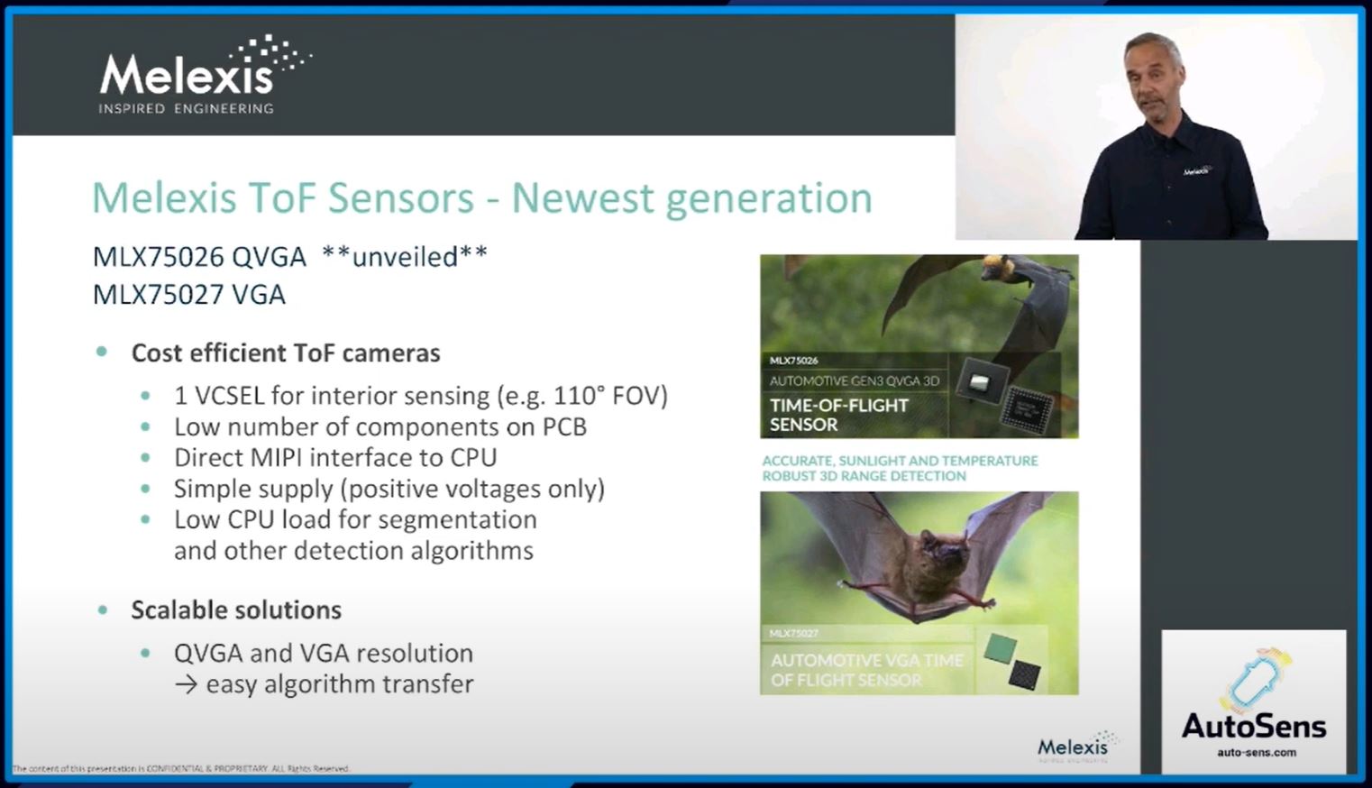
Melexis also announces a QVGA ToF sensor MLX75027 and publishes "ToF Basics" tutorial.
Yole on AI and Mass Surveillance
September 17, 2020 By Leave a Comment
Image Sensors World Go to the original article...
Yole Developpement report "Artificial intelligence and mass surveillance are pushing the camera and computing market to $38B in revenue by 2025" says:"Over the past five years, China has invested heavily in building its mass surveillance system. The development of this “Skynet” network has greatly benefited native Chinese companies HiKVision and Dahua Technologies. In fact, they quickly became #1 and #2, respectively."


Nikon Z 14-24mm f2.8 S review
September 17, 2020 By Leave a Comment
Cameralabs Go to the original article...
The Nikon Z 14-24mm f2.8 S is a professional ultra-wide angle zoom for Nikon’s full-frame Z-series mirrorless cameras. It’s the third native zoom with a fast f2.8 focal ratio and completes the trinity of pro zooms for Nikon's Z system. Check out my full review!…
The post Nikon Z 14-24mm f2.8 S review appeared first on Cameralabs.
Melexis ToF Sensor Presentation
September 17, 2020 By Leave a Comment
Image Sensors World Go to the original article...
Melexis publishes its Autosens September 2020 presentation on driver and in-cabin monitoring with its new ToF QVGA sensor MLX75026:

Nikon Z 50mm f1.2 S review
September 16, 2020 By Leave a Comment
The Nikon Z 50mm f1.2 S becomes the third standard prime lens for Nikon’s full-frame Z-series mirrorless cameras. A popular focal length for street photography and general-purpose use, it features a bright f1.2 focal ratio. Find out if it's right for you in our full review!…
Photron CRYSTA High-Speed 2D Polarization Sensor
September 16, 2020 By Leave a Comment
Image Sensors World Go to the original article...
Photron explains its CRYSTA high-speed 2D polarization camera features and applications:GoPro Hero 9 Black review
September 16, 2020 By 1 Comment
Cameralabs Go to the original article...
The GoPro Hero 9 is the 2020 edition of the popular action camera series that’s also carved a successful niche in the vlogging and webcam Worlds. It’s a rugged block of a camera, waterproof to 10m / 33feet, that now captures 5k video or 20 Megapixel photos, has improved stabilisation and timelapse facilities as well as a new front screen and bigger battery. See it in action in our in-depth review! …
The post GoPro Hero 9 Black review appeared first on Cameralabs.
Ams and Vivo Unveil Broad Collaboration
September 16, 2020 By Leave a Comment
Image Sensors World Go to the original article...
BusinessWire: ams and vivo have collaborated at a strategic technology level for over five years. The collaboration has resulted in several advancements – including Behind OLED (BOLED) display optical and proximity sensing, multi-camera imaging, camera white balance and laser detection auto focus (LDAF) – with joint achievements from the cooperation implemented in many vivo smart phones.With the popularity of 48MP cameras, the problem of slow focus speed has gradually emerged. Ams TMF8801 ToF sensor addresses this by providing accurate measurement in the 2 cm to 2.5 m range.
Mobile phone users increasingly want a full-screen phone. vivo, a leader in display advancements, cooperates extensively with ams to realize technology that optimizes display size – taking full-view display smartphones to a new level. In particular, BOLED display optical and proximity sensors play an important role. ams’ industry leading device sensitivity and supporting software algorithms, combined with sensors optimized to operate BOLED display, bring more full-view display design possibilities to vivo's full-view display smartphone products.
Pinglu Chen, Senior Vice President of Sales and Marketing of Greater China of ams, said:
"We work together with vivo to develop the smartphone sensor technology of tomorrow in the Android market. Through industry-leading optical, proximity, and imaging technologies and solutions in the field of sensors, vivo and ams have created some game-changing technology focused on full-view screens, and advanced smartphone technology and design. In future, we want to further deepen cooperation with vivo and together continue to create products that provide the best-in-class experience for consumers."

Gpixel 16.8M BSI Sensor for Scientific Applications
September 15, 2020 By Leave a Comment
Image Sensors World Go to the original article...
Gpixel announces a new BSI 16.8MP (4096 x 4096) CMOS sensor, GSENSE4040BSI, with 9 μm × 9 μm pixels and an optical area of 36.8mm x 36.8mm. An intra-scene dynamic range of 85 dB is achieved by dual-gain 12bit HDR read out mode, together with a 39 ke– full well capacity and 2.3 e– readout noise. 18 pairs of LVDS channels are used to output data at a maximum frame rate of 24 fps.GSENSE4040BSI is pin compatible with the existing GSENSE4040FSI sensor, but has enhanced imaging performance. The shipments of the new sensor start in October 2020.


Intel LiDAR Teardown Reveals BOM of $35.08
September 15, 2020 By Leave a Comment
Image Sensors World Go to the original article...
TechInsights publishes a teardown of Intel RealSense L515 LiDAR:
"The Intel RealSense L515 is rated for indoor use and can provide depth measurements between 0.25 m and 9 m with a field of view of 70° x 55°. Its LiDAR unit consists of an IR (860 nm) laser reflecting off a scanning MEMS mirror, coupled with an IR photodiode. It is also fitted with an RGB camera which provides a 1080p resolution at 30 fps.
The RealSense L515 is housed in a compact and lightweight “hockey puck” enclosure (61 mm x 26 mm / 100 grams), which makes it ideal for robotics applications, as it can be more easily incorporated into a product."


Samsung Expands its 0.7um Sensor Lineup
September 15, 2020 By Leave a Comment
Image Sensors World Go to the original article...
BusinessWire: Samsung introduces four new Samsung ISOCELL image sensors for its 0.7μm-pixel lineup; 108MP HM2, 64MP GW3, 48MP GM5, and 32MP JD1.
“Samsung continues to pioneer innovations, such as ISOCELL Plus and Smart ISO, to deliver more pixels in a smaller package,” said Yongin Park, EVP of the sensor business at Samsung. “Last year, Samsung introduced the industry’s first 0.7μm-pixel image sensor and the first 108Mp sensors. Now we are bringing more of the advanced pixel technologies to mobile cameras in a variety of options that will enable high-resolution images and sleeker designs in a wider selection of tomorrow’s mobile devices.”
For ultra-high-resolution image sensors, even a mere 0.1μm-difference per pixel can have a significant impact on the overall size of the sensor as well as the height of the camera module. With pixels at 0.7μm, Samsung’s image sensors are up to 15% smaller than the 0.8μm sensors of the same resolution and reduce the height of the camera module by up to 10%.
To collect an ample amount of light and increase the full well capacity, Samsung has incorporated its advanced ISOCELL Plus and Smart-ISO technologies, especially optimized for 0.7μm. ISOCELL Plus retains the received light with a wall-like structure around the pixel while Smart-ISO makes full use of the incoming light by intelligently adjusting the ISO accordingly for optimal exposure.
In the latest 0.7μm products to be introduced later this year, Samsung will start rolling out an enhanced pixel technology, ISOCELL 2.0, which allows excellent performance despite the challenges with decreasing pixel sizes. The new technology further enhanced the wall structure between cells, resulting in added light sensitivity of up to 12 percent compared to the current ISOCELL Plus technology.
The New 0.7μm Lineup;
- ISOCELL HM2 is Samsung’s third 108MP image sensor following the HMX and HM1. The new 108Mp-sensor is around 15% smaller than the 0.8μm-based predecessors, and reduces the height of the camera module by 10%. The HM2 features Super PD, a faster and more effective PDAF, and like the HM1, comes with a nine-pixel binning technology as well as 3x lossless zoom.
- ISOCELL GW3 is a 64MP sensor for mainstream devices. The GW3’s optical size is nearly identical to that of Samsung’s 0.8μm 48MP sensor. In addition to Tetracell and Smart-ISO technologies that help the sensor take bright images with high color fidelity, the GW3 features gyro-based EIS for still photos and videos. The image sensor supports video recording at up to 4K resolution at 60 fps.
- ISOCELL GM5 is a 48MP-image sensor for use in telescoping or ultra-wide angle cameras. When used as a 5x optical telescoping sensor for folded-zoom, the GM5 takes advantage of the 0.7μm pixel size to minimize the camera bulge. For ultra-wide shots, the GM5 supports high-speed full-HD recording at 480fps. The sensor also offers a staggered-HDR feature, a faster and more power-efficient HDR technology that expedites image processing by sending a readout of long, medium, and short exposures of each row of pixels respectively to the mobile processor. As the readout is performed based on Tetracell’s 1.4μm two-by-two pixels, rather than at the individual 0.7μm-pixel level, staggered-HDR can provide brighter and clearer images with less noise.
- ISOCELL JD1 is the industry’s smallest 32MP-image sensor at 1/3.14-inches for smartphones with bezel-less displays that incorporate a hole-in-active-area or motorized pop-up mechanism for the front-facing camera. Like the GM5, the JD1 is also the one the first ISOCELL image sensors to offer staggered-HDR.


Sony A7C review – preview
September 15, 2020 By Leave a Comment
Cameralabs Go to the original article...
The Sony A7C is a mid-range full-frame mirrorless camera with 24 Megapixels, 4k video up to 30p, built-in stabilisation, rangefinder styling and a fully-articulated touchscreen. It’s Sony’s smallest and lightest full-framer to date, packing the photo and movie quality of the A7 III into a more compact body that’s barely larger or heavier than the A6600. Find out more in my preview!…
The post Sony A7C review – preview appeared first on Cameralabs.
Sony Considers Getting License to Keep Selling to Huawei
September 14, 2020 By Leave a Comment
Image Sensors World Go to the original article...
Nikkei Asian Review reports that Sony used to sells billions of dollars worth of smartphone image sensors to Huawei each year. Now, Sony is considering applying for a license to keep selling sensors to the Chinese company.
Sony announces its technology initiatives at the briefing held on Sept. 10. Integrating AI with image sensors is the main initiative in the Imaging and Sensing Division:

FBK MATLAB Model of SPAD-based Flash LiDAR
September 13, 2020 By Leave a Comment
Image Sensors World Go to the original article...
FBK publishes a MDPI paper "Numerical Model of SPAD-Based Direct Time-of-Flight Flash LIDAR CMOS Image Sensors" by Alessandro Tontini, Leonardo Gasparini, and Matteo Perenzoni."We present a Montecarlo simulator developed in Matlab® for the analysis of a Single Photon Avalanche Diode (SPAD)-based Complementary Metal-Oxide Semiconductor (CMOS) flash Light Detection and Ranging (LIDAR) system. The simulation environment has been developed to accurately model the components of a flash LIDAR system, such as illumination source, optics, and the architecture of the designated SPAD-based CMOS image sensor. Together with the modeling of the background noise and target topology, all of the fundamental factors that are involved in a typical LIDAR acquisition system have been included in order to predict the achievable system performance and verified with an existing sensor."


FSI vs BSI PDAF Pixels for 3D Imaging
September 12, 2020 By Leave a Comment
Image Sensors World Go to the original article...
MDPI paper "CMOS Depth Image Sensor with Offset Pixel Aperture Using a Back-Side Illumination Structure for Improving Disparity" by Jimin Lee, Sang-Hwan Kim, Hyeunwoo Kwen, Juneyoung Jang, Seunghyuk Chang, Jongho Park, Sang-Jin Lee, and Jang-Kyoo Shin from from KAIST and Kyungpook National University, Korea, compares FSI and BSI 3D imagers with PDAF pixels:"This paper presents a CMOS depth image sensor with offset pixel aperture (OPA) using a back-side illumination structure to improve disparity. The OPA method is an efficient way to obtain depth information with a single image sensor without additional external factors. Two types of apertures (i.e., left-OPA (LOPA) and right-OPA (ROPA)) are applied to pixels. The depth information is obtained from the disparity caused by the phase difference between the LOPA and ROPA images. In a CMOS depth image sensor with OPA, disparity is important information. Improving disparity is an easy way of improving the performance of the CMOS depth image sensor with OPA. Disparity is affected by pixel height. Therefore, this paper compared two CMOS depth image sensors with OPA using front-side illumination (FSI) and back-side illumination (BSI) structures. As FSI and BSI chips are fabricated via different processes, two similar chips were used for measurement by calculating the ratio of the OPA offset to pixel size. Both chips were evaluated for chief ray angle (CRA) and disparity in the same measurement environment. Experimental results were then compared and analyzed for the two CMOS depth image sensors with OPA."


Cameras Cost 13% of BOM in Samsung Galaxy Note 20 Ultra 5G
September 12, 2020 By Leave a Comment
Image Sensors World Go to the original article...
Counterpoint Research publishes its component analysis of the new Samsung Galaxy Note 20 Ultra 5G. The cameras cost is $60.30 out of the $468 BOM."The device also features one of the most advanced camera sensors in a nicely integrated three-sensor module. Unlike the Galaxy S20 Ultra 5G, the Galaxy Note 20 Ultra 5G features a lower resolution telephoto lens, omitting the DepthVision sensor, and adding a laser auto-focus module optimized for faster focusing. Samsung CIS camera sensors have come a long way and compete fiercely with Sony for design wins," says the company's Senior Analyst, Ethan Qi.

Junction-Free Photovoltaics
September 11, 2020 By Leave a Comment
Image Sensors World Go to the original article...
OSA Optics Express paper "Self-powered broadband photo-detection and persistent energy generation with junction-free strained Bi2Te3 thin films" by Bruno Lorenzi, Yoichiro Tsurimaki, Akihiro Kobayashi, Masayuki Takashiri, and Svetlana V. Boriskina from MIT, University of Milano Bicocca, and Tokai University proposes a way to generate voltage from light with no p-n junction:"We experimentally demonstrate efficient broadband self-powered photo-detection and power generation in thin films of polycrystalline bismuth telluride (Bi2Te3) semiconductors under inhomogeneous strain. The developed simple, junction-free, lightweight, and flexible photo-detectors are composed of a thin active layer and Ohmic contacts on a flexible plastic substrate, and can operate at room temperature and without application of an external bias voltage. We attribute the observed phenomena to the generation of an electric field due to a spontaneous polarization produced by strain gradient, which can separate both photo-generated and thermally-generated charge carriers in bulk of the semiconductor material, without a semiconductor junction. We show that the developed photo-detectors can generate electric power during both the daytime and the nighttime, by either harnessing solar and thermal radiation or by emitting thermal radiation into the cold sky. To the best of our knowledge, this is the first demonstration of the power generation in a simple junction-free device under negative illumination, which exhibits higher voltage than the previously used expensive commercial HgCdTe photo-diode. Significant improvements in the photo-detector performance are expected if the low-charge-mobility polycrystalline active layer is replaced with high-quality single-crystal material. The technology is not limited to Bi2Te3 as the active material, and offers many potential applications in night vision, wearable sensors, long-range LIDAR, and daytime/nighttime energy generation technologies."