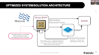
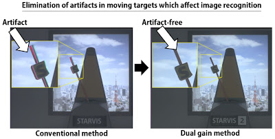
Image Sensors World Go to the original article...
Ibeo publishes a video on LiDAR performance in fog and ways to improve it:
TI video shows an importance of clean power supply for image sensors:
Trioptics publishes its active alignment system video:
EETimes publishes an interview with Omnivision SVP Michael Wu about the company rebranding and latest products & partnership announcements:
ST publishes a video on choosing cover glass for its dToF proximity sensors (a longer version of this video is here):
Gigajot publishes its CTO Jiaju Ma presentation at Photonics Spectra conference: