Archives for November 2020

Samsung Sued by Pictos Over Patent Infringement

Image Sensors World        Go to the original article...

KoreaTimes: Samsung is facing the U.S. International Trade Commission's (USITC) investigation for allegedly infringing on image sensor patents held by Pictos Technologies. This is a fairly long story publicly presented in 2018 by Gil Amelio.

It's not clear what is the relation between the new Pictos and the old image sensor company under the same name that started as Rockwell spin-off and later acquired by ESS. Bloomberg reports that the new Pictos has been formerly known as Imperium IP.

Go to the original article...

UBS: iPhone 12 Pro 3D Cameras Cost 67% of 2D Cameras

Image Sensors World        Go to the original article...

IFNews quotes UBS and Fomalhaut teardown analysis estimating 3D cameras in iPhone 12 Pro and Pro Max cost at 67% and 54% of the cost of 2D cameras, respectively:

UBS poll reveals that smartphone camera spec is rated #12 among the most desirable features. Other image sensor-based features like dual camera, on-display fingerprint, Face ID, and AR/VR functionality are all rated much lower than that:

Go to the original article...

Sony SLVS-EC Article

Image Sensors World        Go to the original article...

Sony publishes an article on its image sensor interface Scalable Low-Voltage Signaling with Embedded Clock, abbreviated SLVS-EC. SLVS-EC is standardized by the Japan Industrial Imaging Association (JIIA). It looks similar to MIPI M-PHY, but has a slower speed of up to 5Gbps per lane.

Go to the original article...

Sony Releases 5um Pixel VGA ToF Sensor

Image Sensors World        Go to the original article...

Sony releases a new 5um BSI ToF sensor - 5um pixel-based IMX570. The new VGA sensor is sampling now with mass production start planned for March 2021.

Go to the original article...

Sony Releases 5um Pixel VGA ToF Sensor

Image Sensors World        Go to the original article...

Sony releases a new 5um BSI ToF sensor - 5um pixel-based IMX570. The new VGA sensor is sampling now with mass production start planned for March 2021.

Go to the original article...

Sony Buys Hundreds of Intel Patents

Image Sensors World        Go to the original article...

IPNewsShots reports that Sony has bought hundreds of Intel patents to protect its image sensor business. Earlier, Sony also has quietly acquired IBM semiconductor patents.

Go to the original article...

iPhone 12 Teardown

Image Sensors World        Go to the original article...

Nikkei and Fomalhaut Techno Solutions tore down the iPhone 12 and iPhone 12 Pro and checked the components origins:
"...the contribution of high-tech Japanese companies remains sizable. Sony is the key supplier for the CMOS image sensors used in iPhone 12 Pro's three camera lenses, including its wide-angle and telephoto lenses, the findings showed. The sensors are priced at around $5.40 to $7.40 each."


iFixit teardown review shows iPhone 12 Max cameras and LiDAR in X-Ray picture:

Go to the original article...

iToF Phase Unwrapping Review

Image Sensors World        Go to the original article...

Chronoptics CTO Refael Whyte publishes an overview of approaches to "Phase Wrapping and its Solution for Indirect Time-of-Flight Depth Sensing" with very nice animations:


Go to the original article...

Characterization of CIS Noise for Automotive Applications

Image Sensors World        Go to the original article...

Institute of Technology Sligo and Waterford Institute of Technology, Irland, publishe a paper "Characterisation of CMOS Image Sensor Performance in Low Light Automotive Applications" by Shane Gilroy, John O'Dwyer, and Lucas Bortoleto.

"The applications of automotive cameras in Advanced Driver-Assistance Systems (ADAS) are growing rapidly as automotive manufacturers strive to provide 360 degree protection for their customers. Vision systems must capture high quality images in both daytime and night-time scenarios in order to produce the large informational content required for software analysis in applications such as lane departure, pedestrian detection and collision detection. The challenge in producing high quality images in low light scenarios is that the signal to noise ratio is greatly reduced. This can result in noise becoming the dominant factor in a captured image thereby making these safety systems less effective at night. This paper outlines a systematic method for characterisation of state of the art image sensor performance in response to noise, so as to improve the design and performance of automotive cameras in low light scenarios. The experiment outlined in this paper demonstrates how this method can be used to characterise the performance of CMOS image sensors in response to electrical noise on the power supply lines."

Go to the original article...

SmartSens Sales Doubled this Year, Expected to Double Again Next Year, IPO Plans

Image Sensors World        Go to the original article...

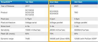
Smartsens has held a Partnership Meeting 2020 (SPM 2020) updating about the company's business and future plans. Smartsens CEO Xu Chen says:

"2020 is an unusual year, but under the influence of the complex international situation and the global epidemic, the overall CIS industry still maintains a growth rate of 20% (data source: Yole)

Dr. Xu Chen pointed out that although next year’s forecasted growth rate has slowed down, Smartsens' overall sales situation still maintains a high-speed growth, and has doubled sales this year, with shipments reaching 220 million units. It is expected that the target set at the beginning of the year will be exceeded, and the sales target of Smartsens will double again next year.

In addition to the repeated increase in sales, Smartsens product line and application areas are also rapidly expanding. The number of Tapeout products has doubled from 13 in 2019 to 26 in 2020, and strives to empower more with excellent CIS imaging technology.

Smartsens' consumer-grade Global Shutter image sensor market, which was laid out in 2017, also achieved good results this year, ranking first in the world in terms of shipments in the consumer-grade machine vision field . And this year's acquisition of Allchip (Shenzhen Anxin Micro) also enabled Smartsens to quickly enter the automotive electronics application field . In addition, just before the SPM 2020 conference, Smartsens released a full range of 2MP-13MP Cellphone Sensor (CS) series of mobile phone application products , officially entering the mobile phone market.

Mr. Chen Xu, Deputy Director of TSMC, gave a speech introducing TSMC’s current latest process R&D and production capacity planning, and said that TSMC will spare no effort to cooperate with Smartsens' growth and development, and also strongly support Smartsens production capacity manufacturing. In the future, TSMC will also work with Smartsens to help China's semiconductor industry chain achieve global cutting-edge quality and maintain a state of sustainable development.

Samsung Semiconductor Executive (Vice President) Mr. Minghui Zhu said in his speech that the cooperation between Samsung and Smartsens is very harmonious and happy, and highly summarized and appreciated the development of Smartsens in recent years with three characteristics. The first is "speed". , I am deeply impressed by Smartsens’s high efficiency; the second is "high and big ", which greatly appreciates its technological innovation ability, and the third is "strategic vision . In the future, Samsung will continue to make efforts to support Smartsens' strategic development and look forward to more future results of joint development with Smartsens.

Next year, Smartsens will celebrate its 10th birthday. On this conference, Dr. Xu Chen announced the three major events of Smarsens' 10th anniversary to the guests. These include the spacious and bright brand-new Smartsens office building that is under design and renovation and will be settled in April next year ; and the new Kunshan test center with a capacity plan of 100kk/month and an area of ​​20 acres that will be completed next year; However, after completing the 1.5 billion pre-ipo round of financing this year, Smartsens will submit a listing application and start the listing plan!"

Go to the original article...

Hole in Pixel Improves NIR Response

Image Sensors World        Go to the original article...

W&WSens Devices, University California at Davis, and University California at Santa Cruz publish a paper "Single Microhole per Pixel in CMOS Image Sensor with Enhanced Optical Sensitivity in Near-Infrared" by E. Ponizovskaya Devine, Wayesh Qarony, Ahasan Ahamed, Ahmed S Mayet, Soroush Ghandiparsi, Cesar Bartolo-Perez, Aly F Elrefaie, Toshishige Yamada, Shih-Yuan Wang, and M. Saif Islam.

"Silicon photodiode based CMOS sensors with backside-illumination for 300 to 1000 nm wavelength range were studied. We showed that a single hole in the photodiode increases the optical efficiency of the pixel. In near-infrared wavelengths, the enhancement allows 70% absorption in a 3 microns thick Si. It is 4x better than for the flat pixel. We compared different shapes and sizes of single holes and holes arrays. We have shown that a certain size and shape in single holes pronounce better optical efficiency enhancement. The crosstalk was successfully reduced with trenches between pixels. We optimized the trenches to achieve minimal pixel separation for 1.12 microns pixel."

Go to the original article...

Infineon Anticipates ToF Camera to Become Standard Feature in Smartphones

Image Sensors World        Go to the original article...

SemiconductorForYou publishes an interview with Philipp von Schierstaedt, SVP RF & Sensors at Infineon. Few quotes:

"We see a development towards 3D ToF image sensors as a standard for high-end smartphones on the front camera – flagship phones are already proving this – and on the rear camera. The fastest growing will surely be the rear camera with above 500 million units/y over the next years. The deployment of 3D sensing technologies will follow this growth as they solve the challenges that new applications set to the rear camera and that traditional 2D technologies fail to accomplish: a real 3D depth map.

Still, challenges exist, for example current commercial devices deploying existing 3D image sensing solutions are not yet able to provide a reasonable resolution without significant trade-offs on extended distance ranges and on the power consumption.

Such shortcomings are now being addressed by the latest 3D ToF imager generations in the REAL3 portfolio of Infineon. Therefore we’re convinced that we will see our new 3D sensor either enabling new classes of applications or taking existing applications to a new level of quality and user experience."

Go to the original article...

Draper Si-Ge-based Single-Photon Detector Gets Award

Image Sensors World        Go to the original article...

Draper reports that its Single Photon Detector (SPD) patent has been awarded by by the Boston Patent Law Association at its 10th Annual Invented Here! event.

Draper’s SPD is intended to be configured in an array of multiple SPDs capable of detecting a single photon with high timing resolution, speed and efficiency over an unparalleled wavelength range, from visible to infrared.

Draper’s SPD uses a silicon-germanium photodiode, which enables detection of the longer wavelengths of light and performance similar to a conventional silicon SPD. It can also function at room temperature. The performance of the new detector is intended to enable ultralow dark-counting rate and timing resolution of better than one nanosecond.

Steven Spector, principal member of Draper’s technical staff, developed the technology with a team at Draper. He said, “Draper’s SPD is so fast and efficient that it can absorb and detect a single particle of light and reset itself for the next one within a nanosecond.

The patent US10636918 "Single electron transistor triggered by photovoltaic diode" presents the idea using a single electron bipolar avalanche transistor (SEBAT) circuit:

"Embodiments of the present invention are directed to a single photon detection circuit that includes a germanium photodiode configured with zero voltage bias to avoid dark current output when no photon input is present and also configured to respond to a single photon input by generating a photovoltaic output voltage and current. A single electron bipolar avalanche transistor (SEBAT) has a base emitter junction connected in parallel with the germanium photodiode and is configured so that the photovoltaic output voltage triggers an avalanche collector current output.

The SEBAT may be formed of silicon material. The germanium photodiode may be formed using germanium material used as deposited plus any dopings and anneals needed to turn it into a photodiode.

Unlike SPADs, which are triggered by single photons, SEBATs are triggered by single electrons. For single electron detection operation, the collector voltage Vcc is set to a high voltage above the breakdown of the collector-base junction. If a negative voltage is applied to the emitter E, the base-emitter junction is forward biased and an emitter current IE appears."

Go to the original article...

ON Semi Presents its SPAD Products for LiDARs

Image Sensors World        Go to the original article...

ON Semi publishes a video on its SPAD products for laser rangefinders and LiDARs:

Go to the original article...

Curved Organic Heterojunction Neuromorphic Image Sensor

Image Sensors World        Go to the original article...

 Nature paper "Curved neuromorphic image sensor array using a MoS2-organic heterostructure inspired by the human visual recognition system" by Changsoon Choi, Juyoung Leem, Min Sung Kim, Amir Taqieddin, Chullhee Cho, Kyoung Won Cho, Gil Ju Lee, Hyojin Seung, Hyung Jong Bae, Young Min Song, Taeghwan Hyeon, Narayana R. Aluru, SungWoo Nam, & Dae-Hyeong Kim (Seoul Institute for Basic Science (IBS), Seoul National University, Gwangju Institute of Science and Technology, and University of Illinois at Urbana-Champaign) sets off a lot of Google News Alerts for me: neuromorphic, organic, curved, heterojunction.

"Conventional imaging and recognition systems require an extensive amount of data storage, pre-processing, and chip-to-chip communications as well as aberration-proof light focusing with multiple lenses for recognizing an object from massive optical inputs. This is because separate chips (i.e., flat image sensor array, memory device, and CPU) in conjunction with complicated optics should capture, store, and process massive image information independently. In contrast, human vision employs a highly efficient imaging and recognition process. Here, inspired by the human visual recognition system, we present a novel imaging device for efficient image acquisition and data pre-processing by conferring the neuromorphic data processing function on a curved image sensor array. The curved neuromorphic image sensor array is based on a heterostructure of MoS2 and poly(1,3,5-trimethyl-1,3,5-trivinyl cyclotrisiloxane). The curved neuromorphic image sensor array features photon-triggered synaptic plasticity owing to its quasi-linear time-dependent photocurrent generation and prolonged photocurrent decay, originated from charge trapping in the MoS2-organic vertical stack. The curved neuromorphic image sensor array integrated with a plano-convex lens derives a pre-processed image from a set of noisy optical inputs without redundant data storage, processing, and communications as well as without complex optics. The proposed imaging device can substantially improve efficiency of the image acquisition and recognition process, a step forward to the next generation machine vision."

Go to the original article...

Sony Promotional Videos: SWIR, Polarization, ToF

Image Sensors World        Go to the original article...

Sony publishes 4 promotional videos about its image sensors: SWIR, polarization sensing, and ToF:

Go to the original article...

LiDAR News: Luminar, Mobileye, Voyant, Tesla, Broadcom, Sense Photonics

Image Sensors World        Go to the original article...

BusinessWire, Forbes: Luminar has struck a deal with Mobileye, an Intel company, to supply Luminar lidar for the company’s Autonomous Vehicle (AV) Series solution in its next phase of driverless car development and testing.

As part of the agreement, Mobileye will collaborate with Luminar to use its lidar for the first generation of its level 4 Mobility-as-a-Service (MaaS) pilot and driverless fleet in key markets around the world, including Tel Aviv, Israel; Dubai, UAE; Paris, France; and Daegu City, South Korea.

Financial terms of the deal aren’t being disclosed. They don’t include Mobileye taking an equity stake in Luminar.

The camera gets you the first 99%” of visual data for self-driving vehicles, says Austin Russell, Luminar CEO. “Lidar gets you that last 1%.” 

Voyant Photonics responds to Elon Mask statement "you need to focus on vision because the entire road system is based on passive optical.

So you have to sell passive optical to have a self-driving system that is generally a solution. And once you solve passive optical, you’ve solved self-driving. So, why bother with anything else?"

Voyant says "nobody drove to work with any electromagnetic radiation coming out their eyes. That is not what eyes do. Yet, anyone who drove in a Tesla was shooting 77 GHz radio waves out of their front bumper.

Teslas have 77 GHz radars from Continental pumping data into their Autopilot systems."

Broadcom presents its LiDAR approach at today's EPIC Online Technology Meeting on 3D Sensing:


Sense Photonics presents its flash LiDAR solution at today's EPIC Meeting:

Go to the original article...

Spying with Vacuum Cleaner LiDAR

Image Sensors World        Go to the original article...

National University of Singapore presents a paper "Spying with your robot vacuum cleaner: eavesdropping via lidar sensors" by Sriram Sami, Yimin Dai, Sean Rui Xiang Tan, Nirupam Roy, and Jun Han.

"This paper presents LidarPhone, a novel acoustic side-channel attack through the lidar sensors equipped in popular commodity robot vacuum cleaners. The core idea is to repurpose the lidar to a laser-based microphone that can sense sounds from subtle vibrations induced on nearby objects. LidarPhone carefully processes and extracts traces of sound signals from inherently noisy laser reflections to capture privacy sensitive information (such as speech emitted by a victim's computer speaker as the victim is engaged in a teleconferencing meeting; or known music clips from television shows emitted by a victim's TV set, potentially leaking the victim's political orientation or viewing preferences). We implement LidarPhone on a Xiaomi Roborock vacuum cleaning robot and evaluate the feasibility of the attack through comprehensive real-world experiments. We use the prototype to collect both spoken digits and music played by a computer speaker and a TV soundbar, of more than 30k utterances totaling over 19 hours of recorded audio. LidarPhone achieves approximately 91% and 90% average accuracies of digit and music classifications, respectively."

Go to the original article...

Best Camera buyers guides

Cameralabs        Go to the original article...

Looking for the best camera, lens or accessories? You've come to the right place! Here you'll find all of my recommended products arranged into categories, whether you're looking for a pocket point-and-shoot or a top-end pro camera for commercial use!…

Go to the original article...

SystemPlus Discovers Samsung ToF Sensor in Meizu Phone

Image Sensors World        Go to the original article...

 SystemPlus publishes a reverse engineering report "3D Time-of-Flight Module in Meizu 17 Pro."

"The 3D sensing module is packaged in one metal enclosure and includes a new Back-side Illumination (BSI) NIR CMOS Image Sensor (CIS) from Samsung. The sensor features 7 µm pixels and a resolution of 0.3 Mpixels. The ToF uses a vertical cavity surface emitting laser (VCSEL) coming from Lumentum.

A wafer level chip scale packaging (WLCSP) driver integrated circuit from PhotonIC generates the pulse and drives the VCSEL’s power and beam shape."

Go to the original article...

Market Forecasts

Image Sensors World        Go to the original article...

MIRAE Asset publishes few slides with the CIS market data:

Go to the original article...

Smartsens Enters Smartphone Market with 2MP-13MP Sensor Lineup

Image Sensors World        Go to the original article...

BusinessWire: Starting from security and surveillance sensors, Smartsens has recently expanded into automotive applications. Now, the company announces plans to penetrate smartphone image sensor market with the CS (Cellphone Sensor) Series products—including the SC200CS-mono, SC200CS-color, SC500CS, SC800CS, and SC1300CS/SC1301CS—covering a range of 2MP to 13MP resolutions to meet a diverse set of applications and customers.

SmartSens is leveraging its proprietary SFCPixel Technology and ultra-low noise reading circuit design in its new smartphone sensors, borrowing from its years of experience in developing superior night vision imaging technology for security devices. These technologies effectively improve performance in low-light environments, allowing smartphone cameras to capture rich and vibrant images under extremely challenging conditions.

The new CS series deliver excellent signal-to-noise ratio. For example, the SC500CS reduces reading noise by over 30% compared with products of the same specifications in the industry while the fixed noise of SC800CS is significantly reduced by 72% with the Max SNR increased by 3dB compared to similar products. Coupled with the signal-to-noise ratio, the noise reduction optimizes for a natural look and feel.

The other standout features of the CS series include the high dynamic range that enables better images in complex light and shadow environments. Compared with the current 60-70dB dynamic range of mainstream smartphone image sensors, the new CS series products can reach over 72dB with a total range more than 6K electrons and the random noise of less than 1.5 electrons. These capabilities allow associated cameras to process images taken in a wide range of lighting conditions, clearly distinguishing the light and dark details.

The sensors also crucially address the emergence of 5G mobile phones and their associated higher power consumption. This is where the CS series excels. The new range benefits from SmartSens’ unique high-end processing and ultra-low power consumption circuit design that reduces sensor power consumption and extends mobile phone standby time without sacrificing the performance.

Our new range of CMOS image sensors takes SmartSens’ expertise and innovation in mission critical camera applications and brings them to one of the most important devices in consumers’ digital lifestyles: the smartphone,” said Yaowu Mo, SmartSens CTO. “The new CS Series image sensors utilize stable technologies from our other lines—including night-vision imaging, excellent noise reduction, PDAF and ultra-low power consumption—to empower advanced smartphone imaging applications and give users an overall better photography experience.

The SC200CS-mono, SC200CS-color, and SC500CS products are now in production. Samples are available for the SC800CS, SC1300CS and SC1301CS.

Go to the original article...

Sony Re-Org

Image Sensors World        Go to the original article...

Sony Semiconductor Solutions announces a re-organization:

  • The platform technology division and the system development organization of each business division will be reorganized and reorganized into the Imaging & Sensing Edge Core Technology Division.
  • A sensor product design department will be newly established by consolidating some of the product design functions of the Imaging Systems Division, Mobile & Sensing Systems Division, and Sony LSI Design Inc.

Go to the original article...

DC Reduction Using Hydrocarbon-Molecular-Ion-Implanted Double Epitaxial Si Wafers

Image Sensors World        Go to the original article...

 MDPI paper "Reduction of Dark Current in CMOS Image Sensor Pixels Using Hydrocarbon-Molecular-Ion-Implanted Double Epitaxial Si Wafers" by Ayumi Onaka-Masada, Takeshi Kadono, Ryosuke Okuyama, Ryo Hirose, Koji Kobayashi, Akihiro Suzuki, Yoshihiro Koga, and Kazunari Kurita from SUMCO, Japan, promises 40% DC improvement, but needs dual layer epi wafers:

"The impact of hydrocarbon-molecular (C3H6)-ion implantation in an epitaxial layer, which has low oxygen concentration, on the dark characteristics of complementary metal-oxide-semiconductor (CMOS) image sensor pixels was investigated by dark current spectroscopy. It was demonstrated that white spot defects of CMOS image sensor pixels when using a double epitaxial silicon wafer with C3H6-ion implanted in the first epitaxial layer were 40% lower than that when using an epitaxial silicon wafer with C3H6-ion implanted in the Czochralski-grown silicon substrate. This considerable reduction in white spot defects on the C3H6-ion-implanted double epitaxial silicon wafer may be due to the high gettering capability for metallic contamination during the device fabrication process and the suppression effects of oxygen diffusion into the device active layer. In addition, the defects with low internal oxygen concentration were observed in the C3H6-ion-implanted region of the double epitaxial silicon wafer after the device fabrication process. We found that the formation of defects with low internal oxygen concentration is a phenomenon specific to the C3H6-ion-implanted double epitaxial wafer. This finding suggests that the oxygen concentration in the defects being low is a factor in the high gettering capability for metallic impurities, and those defects are considered to directly contribute to the reduction in white spot defects in CMOS image sensor pixels."

Go to the original article...

Yole Webinar on Smartphone Camera Trends

Image Sensors World        Go to the original article...

 Yole Developpement webcast "Smartphone Camera Trends" consists of 3 parts:

  1. Yole Développement's Market and Technology brief, reviewing current trends for smartphone cameras.
  2. Beneq presents Atomic Layer Deposition as a uniquely qualified solution to meet advances in wafer level optics, advanced 3D integration, and the perennial need for improved sensor responsivity.
  3. System Plus Consulting presents a reverse costing brief, with the latest evolution of cameras in flagship smartphones and the main players’ technical choices.


Go to the original article...

Canon Licenses Xperi DBI Hybrid Bonding IP to Use in Stacked CMOS Sensors

Image Sensors World        Go to the original article...

BusinessWire: Xperi Holding announces Canon’s license of Invensas DBI hybrid bonding IP portfolio to enhance its image sensors.

Canon is recognized by customers around the world as a long-standing leader in optical and imaging products,” said Craig Mitchell, President of Invensas, a wholly owned subsidiary of Xperi. “We are proud to support Canon’s innovation efforts in the field of image sensors and look forward to expanding our relationship in the future.

Go to the original article...

Assorted News: Omnivision, Sony, ASE, MISIS, Caeleste

Image Sensors World        Go to the original article...

Yuanchuang: Omnivision reports that testing, packaging, and known good wafer reconstruction expenses constitute 9.74% of its image sensor cost.

Digitimes: Sony has added ASE to its backend for automotive CIS supply chain. ASE will set up a new business unit to handle Sony's CIS orders. ASE reportedly has become Sony's second backend partner for processing automotive image sensors, marking its return to the CIS packaging segment following years of hiatus.

PRNewswire: Russian scientists from NUST MISIS National Technological Initiative Center "Quantum Communications" are developing what they call the world's first prototype of an infrared single-photon video detector.

"The detector itself is located inside the cryostat at a temperature of only 2 K, which is close to absolute zero. When a photon is detected, it sends a signal to the processing circuit, and an image appears on the display", comments Grigory Goltsman, Chief Researcher at NUST MISIS NTI Center "Quantum Communications", founder of "Skontel" company.

Caeleste: Bart Dierickx (Co-Founder and CTO) and Ajit Kalgi (Senior Analog Designer) invented a method to increase the charge collection, thus image lag, of a very long narrow photodiode. The N-type pinned photodiode (PPD) itself is constant in width and homogenous in concentration. It is squeezed between two P+ regions, that are at variable distance from the photodiode (Figure 1).

The presence of the P+ region affects the potential in the photodiode, and the construction is so that the potential drops evenly and monotonically, so as to have an effective electric filed in the photodiode that collects the charges (Figure 2).

Go to the original article...

Holy Grail Claim: Perfect RGB‐IR Color Routers Instead of Color Filters

Image Sensors World        Go to the original article...

Wiley Journal of Advanced Photonics Research publishes a paper "Perfect RGB‐IR Color Routers for Sub‐Wavelength Size CMOS Image Sensor Pixels" by Nathan Zhao, Peter B. Catrysse, and Shanhui Fan from Stanford University.

"A critical capability of all image sensors is to separate light into its individual color components. In most technologies today, this is done via color filters. Filters, however, intrinsically waste a large fraction of the light by absorption or scattering. This affects image sensor performance since the amount of light incident on each image sensor pixels reduces quadratically with linear scaling of pixel size. This is particularly detrimental to the performance of (sub‐)wavelength size pixels. In this paper, we provide a conceptually novel approach for color functionality in image sensors, by designing a color router that achieves perfect RGB‐IR color routing for sub‐wavelength size pixels. In a color router, all incident light for each color channel is routed directly and without loss to the photodetector of the corresponding color channel pixel. We show that color routers can be designed to near‐perfectly match a prescribed spectral shape, which is important for color image processing. We further show that we can design these routers to achieve specific spectral bandwidth and to meet angular as well as fabrication constraints. This article is protected by copyright."

Go to the original article...

Airy3D Explains its Technology

Image Sensors World        Go to the original article...

LaserFocusWorld publishes an article "Diffraction mask design brings 3D imaging to standard CMOS image sensors" by Gil Summy (Director, Optics Group) and James Mihaychuk (Product Manager) from AIRY3D, Montreal, QC, Canada.

Airy3D's "DEPTHIQ technology places an optical encoding transmissive diffraction mask (TDM) on a standard CMOS image sensor to generate both high-quality 2D color images and near-field depth maps that are inherently correlated.

The addition of two thin layers of transmissive material, collectively making the TDM, over the top of most CMOS image sensors can provide 3D sensing capabilities with virtually no reduction in 2D image quality. These layers use the process of diffraction from a phase grating to realize compact, low-cost, low-compute solutions for 3D image capture.

The physics underlying the TDM is diffraction from a phase grating. Thus, the TDM is a transparent structure rather than a lossy mask and does not rely on opaque, lithographically patterned features. As such, a TDM can be added to any existing image-sensor design through a small number of postprocessing steps.

Because it is typically only a few microns thick, a TDM can normally be added to an image sensor without requiring changes to the lens or other camera-module components. However, as with any image sensor, it remains important to select a compatible lens in terms of numerical aperture (NA), chief-ray angle (CRA), and alignment tolerancing.

To date, these TDM design approaches have been successfully applied to implement single-sensor 3D imaging solutions based on a wide range of CMOS image sensors. The TDM approach has been adapted to both backside-illuminated mobile sensors for smartphones and frontside-illuminated, global-shutter machine-vision sensors. As such, TDM structures have been incorporated onto sensors having pixel pitches from about 1 to 3 µm and pixel counts from about 2 to 20 Mpixels."

Go to the original article...

css.php