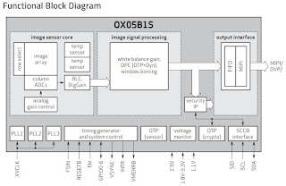
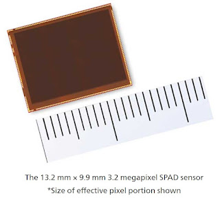
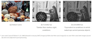
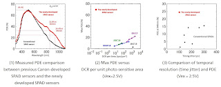
Image Sensors World Go to the original article...
Hong Kong University publishes its video poster on modeling of Current-Assisted Photonic Demodulator (CAPD) for iToF sensors: Almalence demos its super resolution approach with Omnivision endoscopic sensor OVM6948:
Sony AI publishes a video "Imaging & Sensing Project:"
Meere company presents Cube Eye ToF camera capable to operate in 100Klux sunlight:
Imatest publishes a webinar on automotive camera characterization according to P2020 standard:
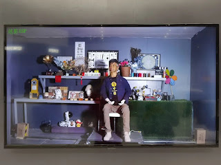
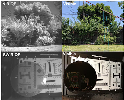
Trieye demos its SEDAR SWIR imaging and ranging technology: