Image Sensors World Go to the original article...
Sony publishes a white paper promoting its InGaAs SWIR sensors:


Visual Industry Guide
Image Sensors World Go to the original article...
Sony publishes a white paper promoting its InGaAs SWIR sensors:Image Sensors World Go to the original article...
MIPI Alliance has recently released the Camera Service Extensions (MIPI CSESM) v1.0 specification, which enhances the MIPI Camera Serial Interface 2 (MIPI CSI-2) image sensor interface with end-to-end functional safety and other features for automotive applications:
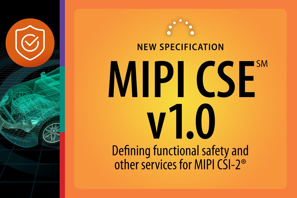
Image Sensors World Go to the original article...
EETimes: Pixart launches Single-Axis Distance Sensor (SAS) product line based on the optical-geometric technology. There are two sensors in the new product line: PAC7088J1 is a middle-range version and PAC7088J2 is s short range one.


Image Sensors World Go to the original article...
Hamamatsu publishes a new flyer for its Orca-Quest qCMOS camera with example applications for its photon resolving capability:


Image Sensors World Go to the original article...
PRNewswire: Xailient announces face recognition AI for Sony's intelligent vision sensor IMX500 with 97.8% accuracy up to 3 meters distance. On the IMX500, Xailient claims to provide the world's most power-efficient Face Recognition AI.

Image Sensors World Go to the original article...
ISSCC publishes its 2022 Agenda. There are 13 image sensor-related papers:
Image Sensors World Go to the original article...
Rice University publishes an OSA Optica paper "EDoF-ToF: extended depth of field time-of-flight imaging" by Jasper Tan, Vivek Boominathan, Richard Baraniuk, and Ashok Veeraraghavan.
Image Sensors World Go to the original article...
During the recent Qualcomm's mobile processor announcements, there was a part on establishing a joint lab with Sony in San Diego working on image sensor and processor co-optimization:
Image Sensors World Go to the original article...
BAE (Fairchild Imaging) presents 12MP 240fps APS-C sensor LTN4625A with global and rolling shutter modes:
Image Sensors World Go to the original article...
GlobeNewswire: Advantest has begun shipping the fourth generation of its high-speed image-processing engine that applies heterogeneous computing technology to detect defects in the data output from CMOS image sensors. When integrated on the proven T2000 ISS platform, the new T2000 IP Engine 4 (Image Processing Engine 4) system provides the means of evaluating the latest high-resolution, high-speed CIS devices used in advanced smart phone cameras.


Image Sensors World Go to the original article...
Qualcomm announces its next generation mobile processor Snapdragon 8 Gen 1:


Image Sensors World Go to the original article...
iNews, Lieyunwang, iFeng: Guangzhou Tyrafos (Chinese name Guangzhou Yinxin Semiconductor Technology Co., Ltd.) announces the A+ round of financing led by Yunqi Capital. By the end of this round of financing, Yinxin Semiconductor is expected to receive hundreds of millions of yuan in the near future.
Tyrafos also announces announced the release of "the world's first non-single photon dToF" (possibly, they mean dToF that is not based on SPADs) and ELISA molecular biological detection solution basedon image sensors.
"The world's first non-single-photon dToF released by Yinxin Semiconductor is the world's first technical solution to achieve direct ToF using CMOS process. Not only the accuracy and resolution are several times higher than the existing SPAD (Single Photon Avalanche Diode) solution. In addition, the overall power consumption of the laser light source at the transmitting end and the sensor at the receiving end has been reduced by 90%, catching up with the core technology of foreign manufacturers such as Apple and STMicroelectronics in this field, and the underlying architecture and circuit IP are independently developed by Yinxin Semiconductor, it solves the technical problem of the neck stuck in the field of 3D perception, and is a milestone breakthrough in the field of 3D perception."


"In the field of fingerprints under the optical screen, Yinxin Semiconductor adopts the innovative design of pixel architecture level to break through the area and cost limits. The chip area is 30%~50% smaller than that of competing products, and the module volume is more than half smaller than that of competing products. It has an ultra-high cost performance. Competitive advantage, in 2019, through cooperation with customers, it became the first optical under-screen fingerprint recognition solution certified by South Korea's Samsung mobile phone. At present, Yinxin Semiconductor has reached an agreement with 4-5 global leading fingerprint solution providers to purchase under-screen fingerprint chips. Intentional orders are expected to contribute hundreds of millions of yuan in revenue."


"The world's first digital ELISA molecular biological detection solution released by Yinxin Semiconductor is the world's first digital solution that directly performs molecular biological detection on the surface of an image sensor. Enzyme Linked Immunosorbent Assay (Enzyme Linked Immunosorbent Assay, abbreviated ELISA or ELASA) refers to a qualitative and quantitative detection method that combines soluble antigens or antibodies on solid-phase carriers such as polystyrene, and uses antigen-antibody specific binding for immunoreaction. . Taking advantage of the company's advantages in high-speed and high-sensitivity image sensors, Yinxin Semiconductor has created a complete set of micro-molecular biological detection equipment based on ELISA standards, achieving a zero breakthrough in this field, and surpassing the United States in detection accuracy and speed. NASDAQ listed company Quanterix (the core technology comes from the Harvard University technical team, the technology founder David Walt is an academician of the American Academy of Engineering and the Medical School, and is also the scientific founder of Illumina) SiMoA (Single-molecule Array) system, and Yinxin Semiconductor In terms of equipment cost and consumables cost, the digital ELISA technology of the company has a significant improvement over Quanterix's SiMoA system technology. The sensitivity of the digital ELISA technology is more than 1000 times higher than that of the traditional ELISA. Its appearance brings protein detection technology directly into the era of single-molecule and digital detection, becoming the true king in the field of fg-level ultra-low abundance protein detection. The optimization of detection accuracy, speed and cost is more conducive to application promotion. In the future, it will have great application potential in the fields of coronavirus detection, influenza virus detection, and early cancer screening."

Tyrafos has been established in May 2019 and its core team coming from TI, Omnivision, Samsung, Himax, TSMC, Mediatek, ASE, Foxconn, and Chi Mei. The company has >90 full-time R&D and operations employees. The core members of the team have 15-20 years experience in the semiconductor industry. The company names Sony and Samsung as its strategic partners, and TSMC, Samsung, and Tower as its foundries.

Image Sensors World Go to the original article...
Lucid Vision Labs publish an explanatory video about Sony IMX490 5.4MP automotive sensor:
Lucid Vision Labs also publishes a measured EMVA1288 performance of the sensor:

Image Sensors World Go to the original article...
Nature paper "Silicon: quantum dot photovoltage triodes" by Wen Zhou, Li Zheng, Zhijun Ning, Xinhong Cheng, Fang Wang, Kaimin Xu, Rui Xu, Zhongyu Liu, Man Luo, Weida Hu, Huijun Guo, Wenjia Zhou & Yuehui Yu from Chinese Academy of Sciences and ShanghaiTech University presents a concept of 1550nm photodetector with internal gain:


Image Sensors World Go to the original article...
Verve.vc publishes an interview with Serguei Okhonin, Actlight CEO and co-founder. Few quotes:
Q: So how does an IP company such as ActLight actually work?
A: We started with an idea and developed it up to the point where we could file patents. The goal, of course, is to license the technology to big semiconductor companies that integrate it into their offering, which they can eventually sell to the big consumer brands we all know. What we do is research and refine our technology to the point that we can provide potential customers with prototypes that should, ideally, convince them of the merits of our sensor. When we achieve this, our job is done. We then basically just provide support.
Q: Let me guess: Convincing big semiconductor companies isn’t that easy.
A: Our potential customers are global market leaders, they have tens of thousands of employees and decades of experience in their field. Now imagine that a small startup from Lausanne comes up to them and says: Look guys, our detector performs better than what you have developed. The first thing they tell you is: That’s impossible. It takes many meetings and a lot of time to convince them otherwise. And then, they do a very thorough due diligence. They will spend more than a year to ascertain the merits of new technology, it is a long process. But once they have done that, and decide to move forward, these companies move very quickly. They have the manpower, the infrastructure, the sales organization, the relationships with their customers… they can bring a product to the mass market at a speed that no startup can match.
Q: Where do you stand in the process you just described?
A: For an IP company like ActLight, the most important achievement is what I call the industrial proof of technology, which means, that a mass-market product incorporates the technology we have developed. We have achieved this milestone now. We licensed our technology to a semiconductor company, the number 1 worldwide, which is building a heart-rate monitor for hearable devices. Thanks to our invention, power consumption is drastically reduced and a high level of miniaturization is achieved. Working samples are already at end customers and, in 2022, mass production starts.
Q: With a use case that will hit the market soon and others that sound promising, ActLight must have appeared on the radar of tech companies by now.
A: After 10 years, we need to think about the future of the company, and there are basically two options. Do we want to grow and pursue more projects, or do we want to sell the company? Recently, we have started to get approached by potential buyers. Of course, such approaches out of the blue need to be examined very well, but it doesn’t surprise me that this happens now.
Q: Because of the traction or what you called industrial proof of technology?
A: Not only that, the M&A activity in the semiconductor industry is incredibly intense at the moment. The sector is red hot. Hardware stocks have reached new highs, and the shortage of semiconductors is talked about a lot. There is an urgency to invest that I haven’t seen in the past 3 decades, it’s insane.
TheBusinessTime publishes an article about Actlight in-ear vital signs monitoring solution.

Image Sensors World Go to the original article...
Techinsights releases a free ebook "The latest development trends in CMOS Image Sensors." This is a recap of a presentation given by Ziad Shukri at IISW 2021:


Image Sensors World Go to the original article...
Sony IMX709 sensor used in the new Oppo Reno 7 smartphone front camera is claimed to be Sony's first sensor based on 22nm process:


Image Sensors World Go to the original article...
Yole Developpement report "ALD equipment market surging with 12% CAGR to reach $680M in 2026, penetrating all More-than-Moore applications" states that CIS is by far the largest market for Atomic Layer Deposition systems:

Image Sensors World Go to the original article...
TheElec: Samsung is to use chip-scale packaging (CSP) to reduce the cost of its low resolution image sensors starting 2022, according to TheElec sources. Currently, Samsung uses chip on board (COB) approach for all sensors.
CSP is done at the wafer level, unlike COB, resulting in increased productivity and lower assembly clean room requirements.
The downside of CSP can only be done in lower resolution image sensors. Most higher resolution image sensors are manufactured with COB. TheElec sources say that CSP can support up to 2MP resolution at as of now.
Image Sensors World Go to the original article...
Korea-based company Syncron presents its first CIS product - 288MP sensor with 3.5um global shutter pixels. Syncron started a long time ago as a spin-off from Kodak Korea and specializes in high-speed and high-resolution industrial digital cameras. The company has been in machine vision camera distribution business, and the new DCS288M sensor appears to be its first CIS product.


Image Sensors World Go to the original article...
EETimes: SK Hynix presents A4C quad pixel PDAF technology:


Image Sensors World Go to the original article...
Harbin Institute of Technology, China, publishes MDPI paper "An Entropy-Based Anti-Noise Method for Reducing Ranging Error in Photon Counting Lidar" by Mingwei Huang, Zijing Zhang, Jiaheng Xie, Jiahuan Li, and Yuan Zhao.


Image Sensors World Go to the original article...
Heriot-Watt University and University of Glasgow publish Journal of Physics paper "Ge-on-Si single-photon avalanche diode detectors for short-wave infrared wavelengths" by Fiona Thorburn, Xin Yi, Zoe Greener, Jaroslaw Kirkoda, Ross Millar, Laura Huddleston, Douglas J Paul, and Gerald S Buller.


Image Sensors World Go to the original article...
Universidad Nacional del Sur (Argentina), Fermi Lab (USA) and Tel Aviv University (Israel) publish an Arxiv.org paper "Smart readout of nondestructive image sensors with single-photon sensitivity" by Fernando Chierchie, Guillermo Fernandez Moroni, Leandro Stefanazzi, Eduardo Paolini, Javier Tiffenberg, Juan Estrada, Gustavo Cancelo, and Sho Uemura.

Image Sensors World Go to the original article...
Facebook-Meta patent application US20210360132 "Stacked Image Sensor with Polarization Sensing Pixel Array" by Manoj Bikumandla, John Enders Robertson, and Andrew Matthew Bardagjy unveils the company's ideas for the sensor for its upcoming AR glasses:


Image Sensors World Go to the original article...
A&S Magazine: InfiRay (former IRay, Chinese name Rui Chuang Wei Na) subsidiary Arrow presents a surveillance camera featuring world's first 2MP 8um pixel InfiRay microbolometer thermal camera combined with 4MP visible one. The 8um thermal sensor has been first announced in April 2021 and is integrated into a production camera now.


Image Sensors World Go to the original article...
Counterpoint Research reports that CIS content per smartphone will expand to an average of 4.1. Despite the global components crunch, CIS growth is expected to grow by double digits to reach almost 6bn units in 2021.
“A big driver has been triple-and-above main camera setups, which accounted for two-thirds of all smartphones sold during the first half,” notes Tarun Pathak, Counterpoint’s director of smartphone research. “What’s really interesting is where a lot of that growth is coming from – Africa, Latin America, India and other emerging markets. As we move through post-COVID upgrade cycles, especially in Android heavy markets, we’re seeing OEMs offer increasingly sophisticated camera hardware to their customers across all segments.”
“High-resolution has also been an area of focus, with 48MP-plus becoming standard. Again, we’re seeing emerging markets lead in growth; and 64MP is starting to become a major segment too. High-res is very important for what is the most hotly contested price band globally – the wholesale $100-$399 category. During the second quarter, two-thirds of devices were high-res and we expect further share increases for the full year.”
“If you’re a product manager today delivering a quad cam device, then you’re probably thinking of configuring wide + ultrawide + macro + depth. But the playing field changes quickly, and we’re likely to see macro and ultrawide merge, leaving room for even more options like telephoto or time-of-flight. Increasing choice and complexity is why algorithm development has become such a critical factor in the success of camera systems,” states Ethan Qi, Counterpoint’s lead camera components analyst.

Image Sensors World Go to the original article...
TalkAndroid, GSMArena: Mediatek presents a 4nm Dimensity 9000 application processor for future smartphones with quite impressive imaging features:


