Assorted News: Omnivision, Audi, AEye, Sense Photonics, ADI

Image Sensors World        Go to the original article...

Digitimes expects Omnivision to enjoy the high-resolution CIS boom starting later in 2020 on rising the popularity of high-spec smartphones and other mobile devices. China-based smartphone manufacturers will be aggressively promoting high-spec smartphones at more affordable prices later in 2020, the newspaper's sources tell.

Other than having production-ready 48MP and 64MP products in its portfolio, Omnivision is a part of Shanghai-based Will Semiconductor now. As such, Omnivision is expected to be be among the beneficiaries of China's push to self-sufficiency in semiconductors, Digitimes sources say.

Another Digitimes article says that GM, Ford, Hyundai, and Volkswagen are to roll out robotaxis (with Level 4-5 autonomous driving) with LiDARs in 2020-2022, while Honda, Lexus, BMW, and Volvo are developing Level 3 autonomous vehicles with LiDAR. This indicates LiDAR will become a standard spec for Level 3 and above autonomous vehicles.

Audi is contemplating cancelling its Level 3 vehicles as the regulations governing autonomous vehicles have yet to be adopted or revised in many countries. Japan has allowed Level 3 autonomous cars to run on roads in the country starting April 2020, and the US, China and European Union have not readied their relevant regulations.

BusinessWire: AEye announced that their 4Sight M 1550nm LiDAR combo has established a new standard for sensor reliability. In testing completed at NTS the 4Sight M scan block surpassed automotive qualification for both shock and vibe. The results of the test showed a 4Sight Sensor can sustain a mechanical shock of over 50G, random vibration of over 12Grms (5-2000Hz), and sustained vibration of over 3G.

The size of the mirror in a MEMS largely determines its reliability. Larger mirrors also have larger inertia, generating 10x to 600x more torque from shock and vibration events. In addition, larger mirrors do not allow for fast, quasi-static movement for agile scanning, which is key to intelligent and reliable artificial perception. Learn more here.

The unique system design of AEye’s MEMS allows a mirror that is less than 1mm in size. Other LiDAR systems use 3mm to 25mm mirrors – which equates to 10X – 600X larger surface area.


Forbes publishes an interview with Shauna McIntyre, new CEO at Sense Photonics:

"A phrase she likes to repeat is “hardware is the gateway.” It’s the combination of Sense’s hardware and software that’s challenged the notion of the stereotypical big rotating unit on the top of autonomous vehicles when one thinks about LiDAR- the laser radar sensing system most automakers install on their autonomous vehicles.

Sense’s system, called Flash LiDAR, is solid state and has no moving parts or spinning coffee can-like devices atop a vehicle. The laser emitter and detector are separate, small units that can be embedded into a vehicle’s design. For instance, the emitter can be hidden behind a headlight and the detector behind the windshield.
"


ADI presents its demo board for Panasonic ToF CCD:

Go to the original article...

Trieye Officially Announces its CMOS SWIR Camera

Image Sensors World        Go to the original article...

Evertiq: TriEye has officially revealed Sparrow – its first CMOS-based SWIR camera. Among the companies that are collaborating with TriEye and are evaluating the Sparrow is DENSO, in addition to Porsche that made an investment in the company back in 2019.

The sensor is particularly effective in low visibility conditions such as identifying black ice, dark clothed pedestrians, and cyclists - all under low-light or other common low visibility conditions, detection scenarios that are paramount for the automotive industry.

We are proud and delighted to announce our collaboration with DENSO which marks a meaningful step forward in delivering our mission of solving the low visibility challenge,” says Avi Bakal, TriEye’s Co-Founder and CEO. “The joint work has been greatly beneficial since day one, bringing together DENSO’s innovative approach and market experience with TriEye groundbreaking technology.

TriEye aims to make SWIR cameras affordable and accessible for the global mass market. The release of Sparrow marks a major milestone towards that goal. The company is expected to launch the first samples of Raven, said to be the world's first CMOS-based SWIR HD camera, later this year.

TriEye’s SWIR camera can be integrated as a standard visible camera and can reuse existing visible image AI algorithms, which saves the effort of recollecting and annotating millions of miles.

Go to the original article...

IC Insights: CIS Market to Drop by 4% This Year, then to Rise by 15% in 2021

Image Sensors World        Go to the original article...

IC Insights forecasts:

"The fallout from the Covid-19 virus crisis in 2020 is expected to lower CMOS image sensor sales for the first time in 10 years, but new record-high revenues are seen next year.

Driven by camera phones and the rapid spread of new embedded applications, CMOS image sensors were the fastest growing semiconductor product category in the last decade with sales quadrupling between 2010 and 2019 to reach $18.4 billion last year. CMOS image sensors set nine consecutive record-high sales levels in the last nine years, but that streak is expected to end in 2020 with revenues falling 4% and unit growth being nearly flat as a result of the economic fallout from the Covid-19 virus crisis and a global recession.

CMOS image sensor sales are forecast to drop to $17.8 billion in 2020 after surging 30% in 2019, according to IC Insights. CMOS image sensor sales rebounding 15% in 2021 to reach a new all-time high of $20.4 billion. The report’s forecast assumes containment of the coronavirus occurs by mid-year and market demand gradually recovering during the second half of 2020.

Between 2019 and 2024, CMOS image sensor revenues are projected to increase by a compound annual growth rate (CAGR) of 7.2% to $26.1 billion in the final year. During last decade (2010-2019), CMOS image sensor sales climbed by a CAGR of 16.9%, rising from $4.5 billion 10 years ago to $18.4 billion last year. In that same timeframe, microprocessor sales grew by a CAGR of 5.9%, NAND flash memories increased by a rate of 7.8%, non-optical sensors were up by 10.0%, and the total semiconductor market expanded by an annual rate of 3.7%. Only pressure sensors (which include MEMS microphone chips) had a CAGR sales growth rate nearly matching CMOS image sensors in the 2010-2019 period.

In the first 10-15 years of this century CMOS image sensor sales growth was mostly fueled by higher volume shipments of camera-equipped cellphones, but this wave began to slow with the saturation of the mobile phone market. In the last decade, a new round of growth took off from the spread of embedded digital imaging systems, including more cameras for automotive safety and driver-assist capabilities in vehicles, machine vision for built-in automation and system intelligence, medical applications, human and face recognition, wearable cameras, 3D video, virtual/augmented reality, and other uses beyond camera phones and stand-alone cameras. On top of that, more digital cameras with fast high-resolution CMOS sensors are also being packed in a growing number of smartphones.
"

Go to the original article...

Tamron 28-200mm f2.8-5.6 Di III RXD review

Cameralabs        Go to the original article...

The Tamron 28-200mm f2.8-5.6 Di III RXD is an all-in-one zoom for Sony’s full-frame mirrorless cameras. It's lighter and more affordable than having both Tamron's 28-75mm f2.8 and 70-180mm f2.8, albeit lacking the constant f2.8 aperture. Find out how it compares to rival super-zooms in our full review!…

The post Tamron 28-200mm f2.8-5.6 Di III RXD review appeared first on Cameralabs.

Go to the original article...

SK Telecom Expands Use Cases for Image Sensor-based RNG

Image Sensors World        Go to the original article...

The Korea Herald: SK Telecom has signed contracts with major IT firms to develop security products for self-driving vehicles, IoT devices and smartphones using its new image-sensor-based security chipset. Names of the partners were not disclosed.

SK Telecom’s QRNG chipset features impenetrable encryption, the company said during a press event. The system, patented by Swiss-based ID Quantique, cannot be breached by computer logic as the codes are created by random movements of photons that travel between an LED light source and a CMOS image sensor equipped in the chipset designed together with fabless Korean company Btree.

The QRNG can become an alternative encryption system in the advent of quantum computers, which can easily decode existing encryption systems,” said Uhm Sang-yun, ID Quantique’s Korean branch manager. The chipset can also process 256,000 keys per second to encrypt and decrypt data or files -- a much larger capacity than existing 128-bit encryption.

Go to the original article...

Sony Adds SNR1s Metric to All Starvis Sensors

Image Sensors World        Go to the original article...

Sony has added SNR1s figures to its table of security and surveillance sensors:

Go to the original article...

Image Sensor in Every Finger

Image Sensors World        Go to the original article...

Karlsruhe Institute of Technology, Germany, publishes a paper "A Soft Humanoid Hand with In-Finger Visual Perception" by Felix Hundhausen, Julia Starke, and Tamim Asfour.

"We present a novel underactued humanoid five finger soft hand, the KIT softhand, which is equipped with cameras in the fingertips and integrates a high performance embedded system for visual processing and control. For efficient on-board parallel processing of visual data from the cameras in each fingertip, we present a hybrid embedded architecture consisting of a field programmable logic array (FPGA) and a microcontroller that allows the realization of visual object segmentation based on convolutional neural networks. Finally, we evaluate the accuracy of visual object segmentation during the different phases of the grasping process using five different objects. Hereby, an accuracy above 90 % can be achieved."

Go to the original article...

Tower Licenses Xperi Patents for 3D Stacked Image Sensors with 2.5um Per-Pixel Interconnect

Image Sensors World        Go to the original article...

BusinessWire: Xperi Holding and Tower announce Tower’s license of Invensas ZiBond and DBI 3D semiconductor interconnect technologies. This technology complements Tower’s stacked wafer BSI sensor platforms for ToF, industrial global shutter and other CMOS image sensors on 300mm and 200mm wafers.

With our fast portfolio expansion, Xperi’s leadership in direct and hybrid bonding technologies enables us to support the rapidly evolving requirements of our customer base as they develop next-generation applications,” said Avi Strum, SVP and GM of the Sensors Business Unit, Tower. “3D stacking architectures and integration are core to our strategy of providing the highest value, proven analog semiconductor solutions, including event-driven and time of flight sensors for mobile, automotive, industrial and high-end photography applications.

With the recently released full design kit for hybrid bonding, Tower’s customers can now design their products on two different wafers, an imager wafer and a mixed-signal CMOS wafer, that are then stacked together with electrical connections on a pixel level, from 10um pitch for applications such as dToF and event-driven sensors, down to 2.5um and even below for applications such as mobile ToF for face recognition applications. This separation into two wafers allows high speed circuitry on the CMOS side, with high sensitivity pixels, due to BSI, and low dark current, below 1 electron/sec per square micron at 60 degrees Celsius, on the imager side. Tower’s unique platform also allows the use of different Epi thicknesses for near infrared sensitivity enhancement.

Tower Semiconductor continues to strengthen its position as a leading and trusted analog foundry partner of customers around the world,” said Craig Mitchell, President of Invensas, a wholly owned subsidiary of Xperi. “Our ZiBond and DBI technologies support the manufacturing of a wide range of devices. We are excited to partner with Tower Semiconductor to deploy our foundational 3D integration technologies into a range of new sensors, in particular time of flight sensors, which we anticipate will be increasingly utilized in automotive, mobile and industrial applications. This partnership continues the strong momentum Xperi has enjoyed as manufacturers worldwide position themselves to address an evolving range of industry needs.

Go to the original article...

IDTechEx Predicts Rise of Organic Image Sensor Market

Image Sensors World        Go to the original article...

PRNewswire: IDTechEx report "Printed and Flexible Sensors 2020-2030: Technologies, Players, Forecasts" predicts a bright future for organic image sensors:

"Hybrid Image Sensors

Hybrid image sensors are an especially promising category. They comprise of a thin film (a few 100 nm) of either an organic semiconductor or quantum dots printed over a silicon readout circuit. They offer three distinct value propositions over the incumbent silicon CMOS detectors: a tuneable bandgap to enable NIR and SWIR imaging at much longer wavelengths, voltage-dependent sensitivity that enables spatially-variable neutral density filter, and more rapid charge collection that facilitates a global rather than rolling shutter.

Critically, hybrid image sensors can be manufactured using repurposed CMOS lines, substantially reducing capital requirements, and facilitating more rapid adoption. The OPD-on-CMOS technology is set to be launched imminently in broadcast cameras, while the QD-on-CMOS technology is already commercially available and will transition to higher-power out-door applications as the thermal and light flux stability of the material system evolves over time. Therefore, the technology can migrate from indoor low-light inspection to outdoor applications such as SWIR imaging for autonomous vehicles.

This disruptive hybrid approach meets genuine market needs, demonstrating that integrating printable, functional materials with standard technology and manufacturing methods can enable substantial performance improvements while lowering adoption barriers.

Large Area Image Sensors

Large area image sensors based on printed organic photodiodes (OPDs) are an innovative technology, representing a complete change from the conventional CMOS-based image detection and going beyond what other large-area image sensors technologies can offer. The technology has two related value propositions: it is flexible and lightweight, unlike large area a-Si image detectors, and in principle it can be printed rapidly at low cost using continuous manufacturing methods.

However, today there are very few manufacturers, and these are mainly targeting biometric sensing as a relatively high value application, thus enabling them to avoid competing with CMOS. In one proposed application, large area under-the-screen image sensors enable 4 fingerprints to be imaged simultaneously, in contrast to the incumbent technology that either images a single finger or requires a complex optical system to image a large area.

While technically impressive, large area image sensing appears to be largely driven by pushing the technology rather than market need. It is questionable whether this capability represents a sufficient advance over incumbent methods to overcome the entry barrier to adoption, especially as fingerprint recognition must compete with incumbent methods.
"

Go to the original article...

3D News: Brookman, LG-Hitachi, Quanergy, Airy3D

Image Sensors World        Go to the original article...

Brookman publishes a video demonstrating its iTOF short-pulse BT008D sensor performance in 100Klux sunlight:


Hitachi-LG demos its 3D people tracker said to be installed in many stores:


Quanergy unveils its QORTEX People counting LiDAR:

"With over 98% accuracy, it will profile each individual without invading privacy and will detect tailgaters or someone It will detect tail gators or anyone coming by.

This particular platform is built with 100% OPA based solid state lidar.
"


Airy3D demos its 3D sensor short range depth map capabilities:


Go to the original article...

Samsung/Sony ToF Camera Cost Estimated at $10.5

Image Sensors World        Go to the original article...

IFNews quotes UBS report on Samsung Galaxy S20 Ultra camera cost analysis. The total cost of the cameras is estimates at $107.5, in line with TechInsights analysis from 3 months ago. The 0.3MP resolution ToF camera cost is estimated at $10.5, less than 10% of the total camera budget, including Sony ToF sensor for $3.

At that cost, the Sony ToF sensor is the cheapest one among all in S20 Ultra:

Go to the original article...

Canon Announces NIR-Enhanced 19um Pixel

Image Sensors World        Go to the original article...

Canon added "CMOS Sensor Products In Development" pages to its image sensor web site. One of them talks about NIR-enhanced version of its 19um pixel sensor:

"By designing a pixel with a deeper well, photons with longer wavelengths can be more efficiently converted into electrons, providing a substantial increase in quantum efficiency (QE) in the Near Infra-Red region. This deeper well resulted in an almost 45% increase in QE at 800nm versus the standard monochrome 19µm pixel size sensor (Canon 35MMFHDXSMA CMOS sensor). Featuring 19µm pixel sizes available in monochrome (35MMFHDXSBM) or with a specialized RGB-NIR color filter array (35MMFHDXSBI), this new family of Canon CMOS sensors allows for expanded possibilities in a wide range of applications."


Another future product is 2.8MP HDR sensor featuring extended operating temperature range:

"In high temperature conditions, the increase in dark current noise adversely affects the quality of the image. The Canon 3U3MRXSAAC sensor is equipped with functionality that mitigates dark current due to increased temperatures, Canon’s sensor is able to maintain high image quality while operating in environments with extreme temperatures ranging from -40°C to 105°C, or -40°F to 221°F."

Go to the original article...

LiDAR News: Ouster, Intel, ADI, TI

Image Sensors World        Go to the original article...

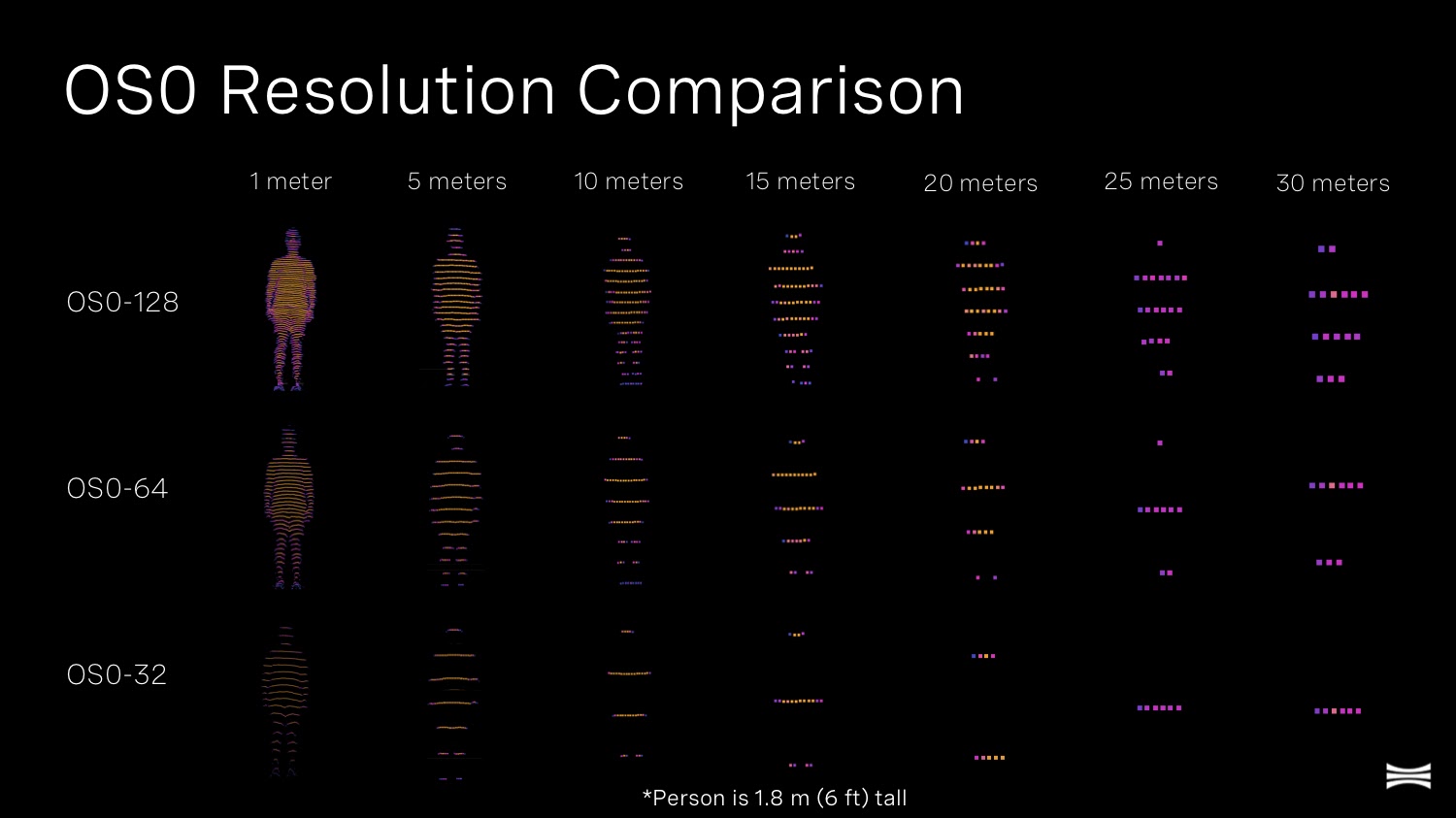
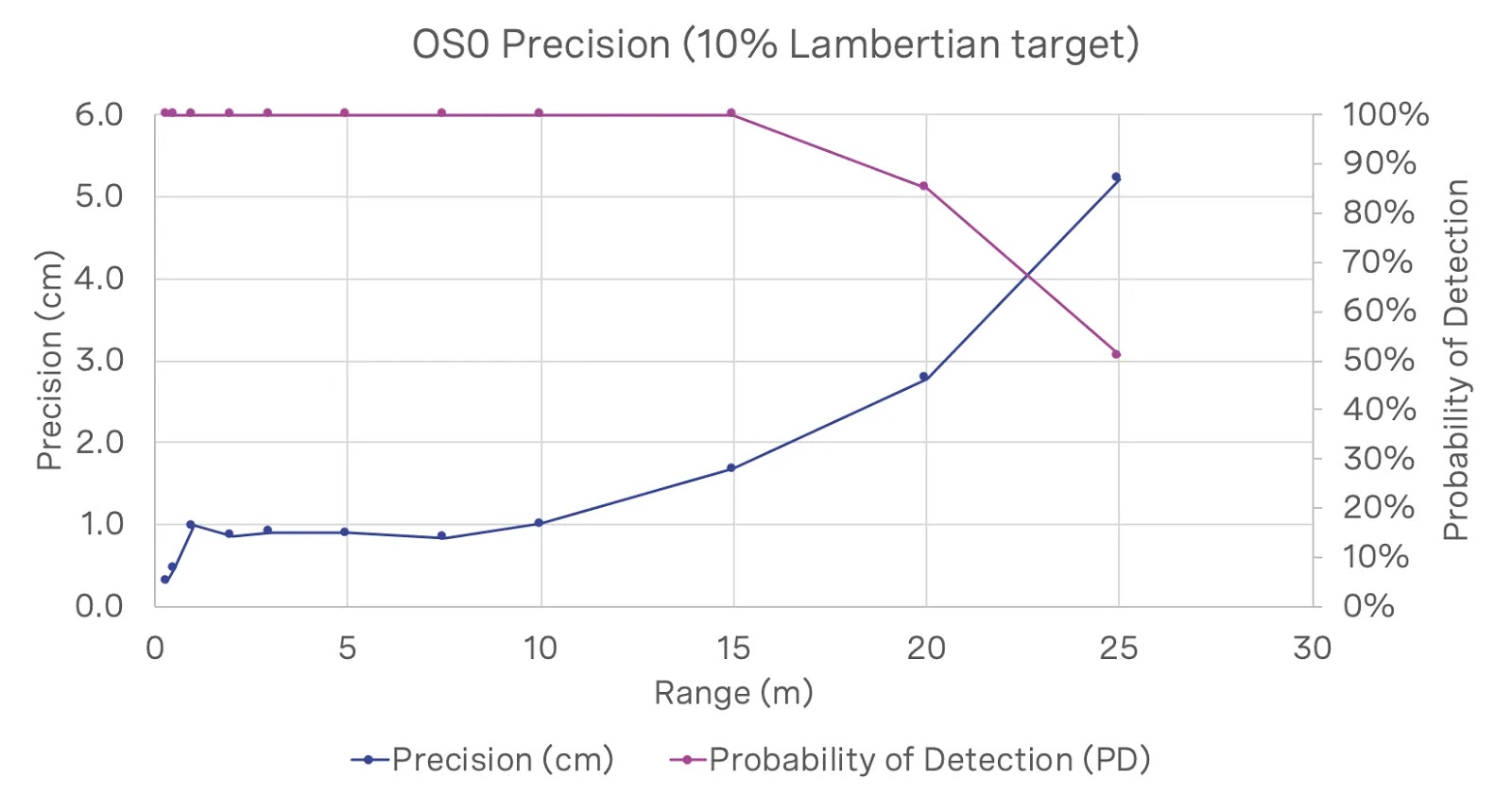
Ouster OS0 LiDAR is optimized for short range applications: "Working with our partner and customers, we identified three attributes (in addition to a wide field of view) that are critical for our customers’ applications: high resolution for object detection, zero centimeter minimum range for maneuvering in close quarters, and high precision for 3D mapping.

The OS0 delivers on all fronts: a 90º vertical field of view, up to 2.6 million points per second (MPS) of resolution, a 0 cm minimum range, and up to millimeter level precision. For customers in AVs, robotics, and mapping who require high performance, the OS0 is the wide-view sensor of choice.

The four key features of the OS0 are:
  1. The 90º wide vertical field of view
  2. 128 channels of resolution
  3. 0 cm minimum range
  4. Millimeter level precision
The OS0 features a minimum range of 0 cm for close range detection. The OS0 achieves this by returning point cloud data for all objects as close as 25 cm to the sensor, and within 25 cm of the sensor the OS0 returns a flag that indicates the presence of an object closer than 25 cm (the flag is not visually represented in the point cloud)."


SPIE publishes Intel presentation "Silicon photonics for LIDAR" by Jonathan K. Doylend talking about Intel attempt to build FMCW automotive LiDAR with SiGe sensing part:


Analog Devices publishes a preliminary spec of its 16-channel TIA for LIDAR applications, ADAL6110, probably going after an 1-channel TI TIA LMH32401:

ADI TIA for LiDARs
TI TIA for LiDARs

Go to the original article...

Large Microlens for SPAD Pixels

Image Sensors World        Go to the original article...

OSA Applied Optics paper "High concentration factor diffractive microlenses integrated with CMOS single-photon avalanche diode detector arrays for fill-factor improvement" by Peter W. R. Connolly, Ximing Ren, Aongus McCarthy, Hanning Mai, Federica Villa, Andrew J. Waddie, Mohammad R. Taghizadeh, Alberto Tosi, Franco Zappa, Robert K. Henderson, and Gerald S. Buller from Heriot-Watt University, UK, and Politecnico di Milano, Italy presents large microlens design attempt:

"Large-format single-photon avalanche diode (SPAD) arrays often suffer from low fill-factors—the ratio of the active area to the overall pixel area. The detection efficiency of these detector arrays can be vastly increased with the integration of microlens arrays designed to concentrate incident light onto the active areas and may be refractive or diffractive in nature.

The ability of diffractive optical elements (DOEs) to efficiently cover a square or rectangular pixel, combined with their capability of working as fast lenses (i.e., ∼?/3) makes them versatile and practical lens designs for use in sparse photon applications using microscale, large-format detector arrays. Binary-mask-based photolithography was employed to fabricate fast diffractive microlenses for two designs of 32×32 SPAD detector arrays, each design having a different pixel pitch and fill-factor. A spectral characterization of the lenses is performed, as well as analysis of performance under different illumination conditions from wide- to narrow-angle illumination (i.e., ?/2 to ?/22 optics).

The performance of the microlenses presented exceeds previous designs in terms of both concentration factor (i.e., increase in light collection capability) and lens speed. Concentration factors greater than 33× are achieved for focal lengths in the substrate material as short as 190µm, representing a microlens f-number of 3.8 and providing a focal spot diameter of less than 4µm. These results were achieved while retaining an extremely high degree of performance uniformity across the 1024 devices in each case, which demonstrates the significant benefits to be gained by the implementation of DOEs as part of an integrated detector system using SPAD arrays with very small active areas.
"

Go to the original article...

Automotive DMS Market to Grow

Image Sensors World        Go to the original article...

ResearchInChina's "Automotive DMS (Driver Monitoring System) Research Report, 2019-2020" forecasts a sharp growth of this market:

"Active DMS, generally enabled by cameras and near-infrared technology, detects the driver's state from eyelid closure, blinking, gaze direction, yawning, and head movements.

In 2006, the Lexus LS 460 was packed with active DMS for the first time, and the camera was mounted on the top of the steering column cover with six built-in near-infrared LEDs. Automakers are not interested in active DMS, because they believe that it increases the cost of the vehicle and consumers may be reluctant to pay for it. Yet, a train of accidents over the recent years highlight the importance of DMS in ADAS, especially L2/L3. Active DMS started to soar from 2018, with the massive availability of the L2 system and the to-be-spawned L3 system.

Euro-NCAP issued a roadmap for 2025, which requires that new cars must be equipped with DMS from July 2022. China has legislated the mandatory installation of DMS for commercial vehicles, and similar stipulations for passenger cars are just around the corner.

10,170 units of active DMS were installed in new passenger cars in China in 2019, surging by 174% on an annualized basis. In 2020Q1, the installations skyrocketed 360% year-on-year to 5,137 units amid the wide use of active DMS in the models priced between RMB150,000 and RMB200,000 and the adoption by WEY, Xpeng, Geely, to name a few.

Most Tier1 suppliers have launched total DMS solutions, including Valeo, Bosch, Continental, Denso, Hyundai Mobis, Visteon, Veoneer, etc. Among Chinese companies, the DMS of Hikvision, SenseTime, Baidu, and Dahua Technology have been found on various brand models.

DMS is used mainly to monitor drivers’ fatigue and distraction. Yet a larger number of sensors, vision + infrared cameras, and even radars mean availability of more functions, e.g., face recognition, age and gender recognition, emotion recognition, seat belt detection, posture, position and forgetting detection, cabin abnormality detection, and infant detection. Face, gender and expression recognition helps with identity authentication and offers richer interaction between human and vehicle.
"

Go to the original article...

Sony Shows Edge AI Processing Examples

Image Sensors World        Go to the original article...

Sony publishes a couple of examples of its edge AI processing:


Go to the original article...

EETimes on iPad Pro LiDAR: Apple Sparked a Race to LiDAR Scanners

Image Sensors World        Go to the original article...

EETimes reporter Junko Yoshida publishes an article "Breaking Down iPad Pro 11’s LiDAR Scanner" derived from an interview with SystemPlus and Yole Developpement analysts:


"Apple has sparked a race to use LiDAR scanners. Apple built one into its iPad Pro 11, and now it seems everyone wants one in their products.

What makes this LiDAR scanner significant — and why other mobile device vendors, including Huawei and Vivo, appear going after it — is a specific technology used inside the unit to sense and measure depth.

In EE Times’ interview, Sylvain Hallereau, senior technology and cost analyst at System Plus, explained that iPad Pro 11’s “LiDAR scanner” consists of an emitter — a vertical cavity surface emitting laser (VCSEL) from Lumentum, and a receptor — near infrared (NIR) CMOS image sensor that does direct measurement of time of flight, developed by Sony.

Sony integrated the NIR CMOS image sensor with SPAD using 3D stacking for ToF sensors for the first time. In-pixel connection made it possible to put the CMOS image sensor together with the logic wafer. With the logic die integrated, the image sensor can do simple calculations of distance between the iPad and objects, Hallereau explained.

Sony has elbowed its way into the dToF segment by developing this new generation SPAD array NIR CMOS image sensor featuring 10 µm size pixels and a resolution of 30 kilopixel.
"

Go to the original article...

EETimes on iPad Pro LiDAR: Apple Sparked a Race to LiDAR Scanners

Image Sensors World        Go to the original article...

EETimes reporter Junko Yoshida publishes an article "Breaking Down iPad Pro 11’s LiDAR Scanner" derived from an interview with SystemPlus and Yole Developpement analysts:


"Apple has sparked a race to use LiDAR scanners. Apple built one into its iPad Pro 11, and now it seems everyone wants one in their products.

What makes this LiDAR scanner significant — and why other mobile device vendors, including Huawei and Vivo, appear going after it — is a specific technology used inside the unit to sense and measure depth.

In EE Times’ interview, Sylvain Hallereau, senior technology and cost analyst at System Plus, explained that iPad Pro 11’s “LiDAR scanner” consists of an emitter — a vertical cavity surface emitting laser (VCSEL) from Lumentum, and a receptor — near infrared (NIR) CMOS image sensor that does direct measurement of time of flight, developed by Sony.

Sony integrated the NIR CMOS image sensor with SPAD using 3D stacking for ToF sensors for the first time. In-pixel connection made it possible to put the CMOS image sensor together with the logic wafer. With the logic die integrated, the image sensor can do simple calculations of distance between the iPad and objects, Hallereau explained.

Sony has elbowed its way into the dToF segment by developing this new generation SPAD array NIR CMOS image sensor featuring 10 µm size pixels and a resolution of 30 kilopixel.
"

Go to the original article...

Huawei P40 Pro Neural Network vs Super-Resolution Algorithms

Image Sensors World        Go to the original article...

Almalence post compares its super-resolution algorithms with (supposedly) AI-based image enhancement in Huawei P40 Pro flagship smartphone:

"Getting back to the P40 Pro’s [supposedly] neural network, an interesting example below. First of all, the NN did an absolutely fantastic job resolving the hair (look at the areas 1 and 2). This looks like something beyond the normal capabilities of super resolution algorithms, which makes us convinced a neural network was involved.

Exploring the image further, however, we can see that in some areas (e.g. area 3) the picture looks very detailed but actually unnatural (and yes, different from the original), so the NN made a visually nice, but actually a wrong guess. In the area 4, the algorithm “resolved” the eye in a way that it distorted the eyelid and iris geometry, making the two eyes looking at different directions; it also guessed the bottom eyelashes in a way that they look like growing from the eyeball, not the eyelid, which looks rather unnatural.
"

Huawei P40 Pro AI NN processing
Almalence super resolution processing

Go to the original article...

Thesis on Printed Image Sensors

Image Sensors World        Go to the original article...

UCB publishes a 2017 PhD Thesis "Printed Organic Thin Film Transistors, Photodiodes, and Phototransistors for Sensing and Imaging" by Adrien Pierre.

"The signal-to-noise ratio (SNR) from a photodetector element increases with larger photoactive area, which is costly to scale up using silicon wafers and wafer-based microfabrication. On the other hand, the performance of solution-processed photodetectors and transistors is advancing considerably. It is proposed that the printability of these devices on plastic substrates can enable low-cost areal scaling for high SNR light and image sensors.

This thesis advances the performance of printed organic thin film transistor (OTFT), pho- todiode (OPD), and phototransistor (OPT) devices optimized for light and image sensing applications by developing novel printing techniques and creating new device architectures. An overview is first given on the essential figures of merit for each of these devices and the state of the art in solution-processed image sensors. A novel surface energy-patterned doc- tor blade coating technique is presented to fabricate OTFTs on flexible substrates over large areas. Using this technique, OTFTs with average mobility and on-off ratios of 0.6 cm^(2)/Vs and 10^(5) are achieved, which is competitive with amorphous silicon TFTs.

High performance OPDs are also fabricated using doctor blade coating and screen printing. These printing pro- cesses give high device yield and good controllability of photodetector performance, enabling an average specific detectivity of 3.45×10^(13) cm·Hz^(0.5)·W^(-1) that is higher than silicon photo- diodes (10^(12-13)).

Finally, organic charge-coupled devices (OCCDs) and a novel OPT device architecture based on an organic heterojunction between a donor-acceptor bulk heterojunction blend and a high mobility semiconductor that allows for a wide absorption spectrum and fast charge transport are discussed. The OPT devices not only exhibit high transistor and photodetector performance, but are also able to integrate photogenerated charge at video frame rates up to 100 frames per second with external quantum efficiencies above 100%. Applications of these devices include screen printed OTFT backplanes, large-area OPDs for pulse oximeter applications, and OPT-based image sensors.
"

Go to the original article...

Analog CNN Integration onto Image Sensor

Image Sensors World        Go to the original article...

Imperial College London and Ryerson University publish Arxiv.org paper "AnalogNet: Convolutional Neural Network Inference on Analog Focal Plane Sensor Processors" by Matthew Z. Wong, Benoit Guillard, Riku Murai, Sajad Saeedi, and Paul H.J. Kelly.

"We present a high-speed, energy-efficient Convolutional Neural Network (CNN) architecture utilising the capabilities of a unique class of devices known as analog Focal Plane Sensor Processors (FPSP), in which the sensor and the processor are embedded together on the same silicon chip. Unlike traditional vision systems, where the sensor array sends collected data to a separate processor for processing, FPSPs allow data to be processed on the imaging device itself. This unique architecture enables ultra-fast image processing and high energy efficiency, at the expense of limited processing resources and approximate computations. In this work, we show how to convert standard CNNs to FPSP code, and demonstrate a method of training networks to increase their robustness to analog computation errors. Our proposed architecture, coined AnalogNet, reaches a testing accuracy of 96.9% on the MNIST handwritten digits recognition task, at a speed of 2260 FPS, for a cost of 0.7 mJ per frame."

Go to the original article...

Thesis on SWIR Thin Film Sensor Optimization

Image Sensors World        Go to the original article...

MSc Thesis "Optimization of Short Wavelength Infrared (SWIR) Thin Film Photodetectors" by Ahmed Abdelmagid from University of Eastern Finland and imec explains quantum dot sensors trade-offs in SWIR band:

"Quantum dots (QDs) can be a promising candidate to realize low-cost photodetectors due to its solution processability which enables the use of economical deposition techniques and the monolithic integration on the complementary metaloxide-semiconductor (CMOS) readout. Moreover, the electronic properties of QDs are dependent on both QD size and surface chemistry. Modification of quantum confinement provides control of the QD bandgap, ranging form from 0.7 to 2.1 eV which make it ideal candidate for the detection in the SWIR region. In addition, by selecting the appropriate ligand, the position of the energy levels can be tuned and therefore, n-type or p-type QDs can be achieved."

Go to the original article...

ResearchInChina: Automotive Thermal Cameras are Too Expensive for Mass Market Cars

Image Sensors World        Go to the original article...

ResearchInChina publishes a report "Automotive Infrared Night Vision System Research Report, 2019-2020."

"Cadillac equipped its sedans with night vision systems early in 2000, being the world’s first to pioneer such system. Mercedes-Benz, BMW, Audi, etc. followed suit. By 2013, a dozen OEMs had installed night vision systems on their top-of-the-range models but having sold not so well to this day due to the costliness of the night vision system.

4,609 new passenger cars carrying night vision systems were sold in China in 2019, an annualized spurt of 65.6% thanks to the sales growth of Cadillac XT5, Cadillac XT6 and Hongqi H7, according to ResearchInChina.

Veoneer is a typical trailblazer that has spawned infrared night vision systems in the world, and its products have experienced four generations. Its 4th-Gen night vision system, expected in June 2020, will have improved field of view and detection distances, reduction in size, weight and cost featuring enhanced algorithms for pedestrian, animal and vehicle detection as well as supporting night time automatic emergency braking (AEB) solutions.

Boson-based thermal sensing technology from FLIR Systems has been adopted by Veoneer for its L4 autonomous vehicle production contract, planned for 2021 with a “top global automaker”. Veoneer’s system will include multiple thermal sensing cameras that provide both narrow and wide field-of-view capabilities to enhance the safety of self-driving vehicles, and that help detect and classify a broad range of common roadway objects and are especially adept at detecting people and other living things.

FLIR has been sparing no effort in the availability of infrared thermal imaging technology in automobiles. In August 2019, FLIR announced its next-generation thermal vision Automotive Development Kit (ADK) featuring the high-resolution FLIR Boson thermal camera core with a resolution of 640 × 512 for the development of self-driving cars.

Uncooled infrared imagers and detector technology remain hot in research to date In August 2019, IRay Technology released a 10-μm 1280 × 1024 uncooled infrared focal plane detector. Maxtech predicts that the unit price of uncooled thermal imaging cameras will be below $2,000 after 2021, and the sales will outnumber 3 million units.

Still, infrared cameras are too expensive for automotive use. Israel-based ADASKY, China's Dali Technology, Guide Infrared and North Guangwei Technology are working on the development and mass production of low-cost infrared thermal imagers.
"

Go to the original article...

MIPI Completes Automotive A-PHY v1.0 Development

Image Sensors World        Go to the original article...

BusinessWire: The MIPI Alliance announces that development has been completed on MIPI A-PHY v1.0, a long-reach SerDes physical layer interface for automotive applications. The specification is undergoing member review, with official adoption expected within the next 90 days.

A-PHY is being developed as an asymmetric data link in a point-to-point topology, with high-speed unidirectional data, embedded bidirectional control data and optional power delivery, all over a single cable. Version 1.0 offers several core benefits:
  • Simpler system integration and lower cost: native support for devices using MIPI CSI-2 and DSI-2, ultimately eliminating the need for bridge ICs
  • Long reach: up to 15 meters
  • High performance: 5 speed gears (2, 4, 8, 12 and 16 Gbps), with a roadmap to 48 Gbps and beyond
  • High reliability: ultra-low 1E-18 packet error rate for unprecedented performance over the lifetime of a vehicle
  • High resilience: ultra-high immunity to EMC effects by virtue of a unique PHY-layer retransmission system

Rick Wietfeldt, Director, MIPI Alliance Board of Directors, presents A-PHY features:

Go to the original article...

MacBook Air battery repair

Cameralabs        Go to the original article...

Has your MacBook battery failed? Is Apple quoting a fortune for a repair, if it's even possible? Find out how I fixed my 2011 MacBook for only $55!…

The post MacBook Air battery repair appeared first on Cameralabs.

Go to the original article...

Princeton Instruments on Imaging Applications in Quantum Research

Image Sensors World        Go to the original article...

Teledyne Princeton Instruments presentation of Imaging Applications in Quantum Research, including the IR-enhances BR_eXcelon CCD with over 35% QE at 1000nm:

Go to the original article...

Plasmonic Metasurface CFA for SPAD Imager

Image Sensors World        Go to the original article...

OSA Optica publishes a paper "Ultralow-light-level color image reconstruction using high-efficiency plasmonic metasurface mosaic filters" by Yash D. Shah, Peter W. R. Connolly, James P. Grant, Danni Hao, Claudio Accarino, Ximing Ren, Mitchell Kenney, Valerio Annese, Kirsty G. Rew, Zoë M. Greener, Yoann Altmann, Daniele Faccio, Gerald S. Buller, and David R. S. Cumming from Glasgow University, Heriot-Watt University, UK and Boise State University, USA.

"We have fabricated a high-transmittance mosaic filter array, where each optical filter was composed of a plasmonic metasurface fabricated in a single lithographic step. This plasmonic metasurface design utilized an array of elliptical and circular nanoholes, which produced enhanced optical coupling between multiple plasmonic interactions. The resulting metasurfaces produced narrow bandpass filters for blue, green, and red light with peak transmission efficiencies of 79%, 75%, and 68%, respectively. After the three metasurface filter designs were arranged in a 64×64 format random mosaic pattern, this mosaic filter was directly integrated onto a CMOS single-photon avalanche diode detector array. Color images were then reconstructed at light levels as low as approximately 5 photons per pixel, on average, via the simultaneous acquisition of low-photon multispectral data using both three-color active laser illumination and a broadband white-light illumination source."

Go to the original article...

Omnivision Announces 140dB HDR Automotive Sensor and DMS Wafer-Level Camera

Image Sensors World        Go to the original article...

BusinessWire: OmniVision announces the OX03C10 ASIL-C automotive sensor that combines a large 3.0um pixel size with HDR of 140dB and the LED flicker mitigation (LFM) for viewing applications with minimized motion artifacts. The new image sensor delivers 1920x1280p resolution at 60 fps with HDR and LFM. Additionally, the OX03C10 is said to have the lowest power consumption of any LFM image sensor with 2.5MP resolution—25% lower than the nearest competitor—along with the industry’s smallest package size, enabling the placement of cameras that continuously run at 60 fps in even the tightest spaces.

Basic image processing capabilities were also integrated into this sensor, including defect pixel correction and lens correction. The integration of OmniVision’s HALE (HDR and LFM engine) combination algorithm uniquely provides top HDR and LFM performance simultaneously.

Many stakeholders in the viewing automotive camera market are asking for higher performance, such as increased resolution, 140dB HDR and top LFM performance,” explained Pierre Cambou, Principal Analyst, Imaging from Yole Développement. “In particular, these performance increases are needed for high end CMS, also called e-Mirror, which is growing in popularity.

The OX03C10 uses our Deep Well, dual conversion gain technology to provide significantly lower motion artifacts than the few competing sensors that offer 140dB HDR,” said Kavitha Ramane, staff automotive product marketing manager at OmniVision. “Additionally, our split-pixel LFM technology with four captures provides the best performance over the entire automotive temperature range. This combination of the industry’s top HDR and LFM with a large 3.0 micron pixel enables automotive viewing system designers with the greatest image quality across all lighting conditions and in the presence of flickering LEDs from headlights, road signs and traffic signals.

OmniVision’s PureCel Plus-S stacked architecture enables pixel performance advantages over non-stacked technology. For example, 3D stacking allowed OmniVision to boost pixel and dark current performance, resulting in a 20% improvement in the signal-to-noise ratio over the prior generation of its 2.5MP viewing sensors. The OX03C10 also features 4-lane MIPI CSI-2 and 12-bit DVP interfaces.

The new OX03C10 image sensor is planned to be AEC-Q100 Grade 2 certified, and is available in both a-CSP and a-BGA packages.


BusinessWire: OmniVision announces the OVM9284 CameraCubeChip module—the world’s first automotive-grade, wafer-level camera. This 1MP module has a compact size of 6.5 x 6.5mm to provide driver monitoring system (DMS) designers with flexibility on placement within the cabin while remaining hidden from view. Additionally, it has the lowest power consumption among automotive camera modules—over 50% lower than the nearest competitor—which enables it to run continuously in the tightest of spaces and at the lowest possible temperatures for maximum image quality.

The OVM9284 is built on OmniVision’s OmniPixel 3-GS global-shutter pixel architecture, which is said to provide best-in-class QE at the 940nm. The new sensor has a 3um pixel and a 1/4" optical format, along with 1280 x 800 resolution.

The accelerated market drive for DMS is expected to generate a 43% CAGR between 2019 and 2025,” asserted Pierre Cambou. “DMS is probably the next growth story for ADAS cameras as driver distraction is becoming a major issue and has brought regulator attention.

Most existing DMS cameras use glass lenses, which are large and difficult to hide from drivers to avoid distraction, and are too expensive for most car models,” said Aaron Chiang, marketing director at OmniVision. “Our OVM9284 CameraCubeChip module is the world’s first to provide automotive designers with the small size, low power consumption and reflowable form factor of wafer-level optics.

The OVM9284’s integration of OmniVision’s image sensor, signal processor and wafer-level optics in a single compact package reduces the complexity of dealing with multiple vendors, and increases supply reliability while speeding development time. Furthermore, unlike traditional cameras, all CameraCubeChip modules are reflowable. This means they can be mounted to a printed circuit board simultaneously with other components using automated surface-mount assembly equipment, which increases quality while reducing assembly costs.


A virtual demo and Q&A for the both new products will be available at AutoSensONLINE’s virtual demo sessions, on Friday, June 12th at 10:40am (Eastern). Registration is free at: ttps://auto-sens.com/autosens-online-tickets

Go to the original article...

200Kfps Sensor Thesis

Image Sensors World        Go to the original article...

University of Nevada at Las Vegas publishes a PhD Thesis "A Highly-Sensitive Global-Shutter CMOS Image Sensor with on-Chip Memory for hundreds of kilo-frames per second scientific experiments" by Konstantinos Moutafis.

"In this work, a highly-sensitive global-shutter CMOS image sensor with on-chip memory that can capture up to 16 frames at speeds higher than 200kfps is presented. The sensor fabricated and tested is a 100 x 100 pixel sensor, and was designed to be expandable to a 1000 x 1000 pixel sensor using the same building blocks and similar architecture.

The heart of the sensor is the pixel. The pixel consists of 11 transistors (11T) and 2 MOSFET capacitors. A 6T front-end is followed by a Correlated Double Sampling (CDS) circuitry that includes 2 capacitors and a reset switch. The 4T back-end circuitry consists of a source follower, in-pixel current source and 2 switches. The pixel design is unique because of the following. In a relatively small area, 15.1um x 15.1um, it performs CDS that limits the noise stored in the pixel memories to less than 0.33mV rms and allows the stored value to be read in a single readout. Moreover, it has in-pixel current source, which can be turned OFF when not in use, to remove the dependency of its output voltage to its location in the sensor. Furthermore, the in-pixel capacitors are MOSFET capacitors and do not utilize any space in the upper metal layers, therefore, they can be used exclusively for routing. And at the same time it has a fill
factor greater than 40%, which important for high sensitivity.

Each pixel is connected to a dedicated memory, which is outside the pixel array and consists of 16 MOSFET capacitors and their access switches (1T1C design). Fifty pixels share a line for their connection to their dedicated memory blocks, and, therefore, the transfer of all the stored pixel values to the on-chip memories happens within 50 clock cycles. This allows capturing consecutive frames at speeds higher than 200 kfps. The total rms noise stored in the memories is 0.4 mV.
"

Go to the original article...

Ricoh WG-70 review

Cameralabs        Go to the original article...

The Ricoh WG-70 is a rugged compact that’s waterproof to 14 metres, can withstand a 1.6m drop and can be used down to -10C. Find out if it's the tough camera for you in our review!…

The post Ricoh WG-70 review appeared first on Cameralabs.

Go to the original article...

css.php