ISSCC 2021: Sony SPAD-Based HDR Sensor

Image Sensors World        Go to the original article...

Sony presents an HDR counter & time stamp-based approach for SPAD sensors:

"A 250fps 124dB Dynamic-Range SPAD Image Sensor Stacked with Pixel-Parallel Photon Counter Employing Sub-Frame Extrapolating Architecture for Motion Artifact Suppression"
by Jun Ogi, Takafumi Takatsuka, Kazuki Hizu, Yutaka Inaoka, Hongbo Zhu, Yasuhisa Tochigi, Yoshiaki Tashiro, Fumiaki Sano, Yusuke Murakawa, Makoto Nakamura, Yusuke Oike.

Go to the original article...

ISSCC 2021: Samsung 0.64um Pixel

Image Sensors World        Go to the original article...

This year, ISSCC has not released its usual media kit with preview snippets of the most interesting papers. So, I'm filling the void with few such snippets. The first one is about Samsung 0.64um pixel:

"1/2.74-inch 32Mpixel-Prototype CMOS Image Sensor with 0.64μm Unit Pixels Separated by Full-Depth Deep-Trench Isolation"
by JongEun Park, Sungbong Park, Kwansik Cho, Taehun Lee, Changkyu Lee, DongHyun Kim, Beomsuk Lee, SungIn Kim, Ho-Chul Ji, DongMo Im, Haeyong Park, Jinyoung Kim, JungHo Cha, Taehoon Kim, In-Sung Joe, Soojin Hong, Chongkwang Chang, Jingyun Kim, WooGwan Shim, Taehee Kim, Jamie Lee, Donghyuk Park, EuiYeol Kim, Howoo Park, Jaekyu Lee, Yitae Kim, JungChak Ahn, YoungKi Hong, ChungSam Jun, HyunChul Kim, Chang-Rok Moon, Ho-Kyu Kang

"...a 0.7μm pixel sensor was demonstrated with acceptable photodiode (PD) full-well capacity (FWC) of >6,000e as well as signal-to-noise ratio (SNR) of ~32dB without optical/electrical crosstalk by employing state-of-the-art full-depth deep-trench isolations (FDTIs). However, further scaling requires elaborate fabrication innovation and layout ideas. At the same time, meeting every aspect of pixel performance compared to the previous generation becomes even more difficult, e.g., with respect to dark or illuminated characteristics, fixed-pattern or temporal noises, etc. The latter, in particular, is associated with in-pixel source-follower (SF) amplifiers. Therefore, electrical performance of scaled in-pixel transistors cannot be overlooked. In this paper, a 32-megpixel (MP) CIS with 0.64μm unit pixels is demonstrated with FDTI design. Innovations in terms of fabrication and design to achieve this performance with scaling are discussed."

Go to the original article...

Ricoh Explains Importance of Low-Ripple Supply for Image Sensors

Image Sensors World        Go to the original article...

Ricoh publishes a video explaining the importance of low ripple supply for CMOS sensors:

Go to the original article...

Pointcloud Inc. and University of Southampton Publish Nature Paper on their Coherent 3D Imager

Image Sensors World        Go to the original article...

A Nature paper "A universal 3D imaging sensor on a silicon photonics platform" by Christopher Rogers, Alexander Y. Piggott, David J. Thomson, Robert F. Wiser, Ion E. Opris, Steven A. Fortune, Andrew J. Compston, Alexander Gondarenko, Fanfan Meng, Xia Chen, Graham T. Reed & Remus Nicolaescu from San Francisco-based Pointcloud Inc. and UK University of Southampton appears to be a minor version of their Arxiv.org paper published in August 2020.

Graham Reed, Professor of Silicon Photonics within the ORC said, “LIDAR has been promising a lot but has not always delivered on its potential in recent years because, although experts have recognised that integrated versions can scale down costs, the necessary performance has not been there. Until now.

The silicon photonics system we have developed provides much higher accuracy at distance compared to other chip-based LIDAR systems to date, and most mechanical versions, showing that the much sought-after integrated system for LIDAR is viable.

Remus Nicolaescu, the CEO of Pointcloud Inc added, “The combination of high performance and low cost manufacturing, will accelerate existing applications in autonomy and augmented reality, as well as open new directions, such as industrial and consumer digital twin applications requiring high depth accuracy, or preventive healthcare through remote behavioural and vital signs monitoring requiring high velocity accuracy."

"Operating at the quantum noise limit, our system achieves an accuracy of 3.1 millimetres at a distance of 75 metres when using only 4 milliwatts of light, an order of magnitude more accurate than existing solid-state systems at such ranges. Future reductions of pixel size using state-of-the-art components could yield resolutions in excess of 20 megapixels for arrays the size of a consumer camera sensor."

Go to the original article...

Samsung Explains its Smart-ISO Pro

Image Sensors World        Go to the original article...

Samsung publishes a promotional video explaining its Smart-ISO Pro feature:

Go to the original article...

Smartsens Presents its Global Shutter Sensor Plans

Image Sensors World        Go to the original article...

EET-China publishes Smartsens article on the company's machine vision sensors evolution:

Go to the original article...

Teledyne Trumpets a New Era in Large Area CMOS Imaging

Image Sensors World        Go to the original article...

GlobeNewsWire: Teledyne Imaging (former Princeton Instruments group) introduces LACera technology said to be "a significant step forward in CMOS capabilities for advanced imaging which will enable the next generation of scientific discovery.

LACera delivers greater than 90% QE and a proprietary low noise global shutter architecture with up to 18-bit readout – a combination of performance not previously available in wafer scale sensors.

LACera technology will be exclusively featured in next generation CMOS cameras to be announced later this year and includes x-ray, EUV and VIS-NIR versions.

Go to the original article...

NIT Announces Novel Stacking Technology for InGaAs to ROIC Bonding

Image Sensors World        Go to the original article...

New Imaging Technologies announces the release of several new SWIR sensors now produced with NIT in-house designed stacking technology, internally named NH.

The NH technology allows to stack a photodiode array (PDA) of InGaAs to a CMOS ROIC at pixel level. The NH technology does not rely on the classical Indium bump hybridization technique, therefore improving the manufacturing yield and lowering the sensor cost.

The VGA line of SWIR products with 15µm pitch is already in full production since several years using the NH technology.  New products with higher resolution and lower pitch from 10µm down to 7.5µm are currently under qualification, such as an HD array (1280×1024 pixels @ 10µm)

The roadmap towards very small pitch <5µm and Full HD+ formats is under construction at NIT.

Go to the original article...

ON Semi Unveils Low Power Smart Shot Camera

Image Sensors World        Go to the original article...

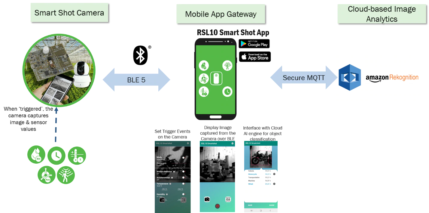
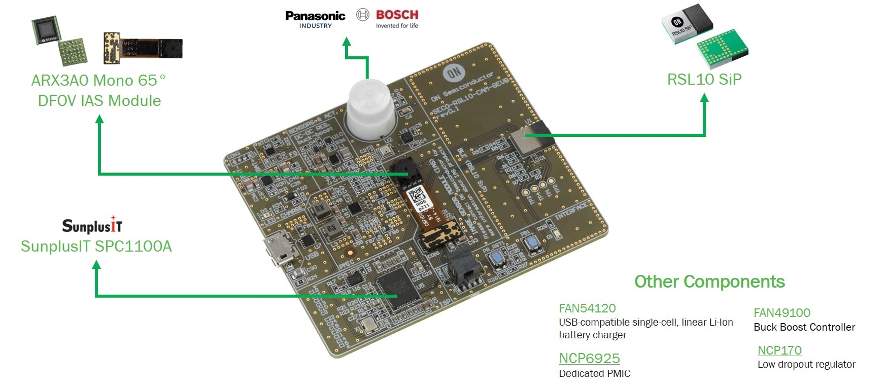
BusinessWire: ON Semiconductor introduces the RSL10 Smart Shot Camera, combining cloud-based AI with ultra-low-power image capture and recognition for IoT endpoints. The camera is based on ARX3A0 CMOS sensor with 560 x 560 pixel resolution, 2.2um pixel size, and a frame rate up to 360 fps. The sensor has an innovative super low power mode which draws less than 3.2 mW while active, and can detect motion or changes in lighting conditions and wake the rest of the system up.

Go to the original article...

Albert Theuwissen Delivers Keynote at IEEE Sensors 2020: DTI is Here to Stay!

Image Sensors World        Go to the original article...

Albert Theuwissen delivered a keynote at 2020 IEEE Sensors conference titled "Deep-Trench Isolation is Here to Stay!" Below is a video recording of the keynote:

Go to the original article...

SMIC to Benefit from Increased Demand to its 40nm and 65nm CIS Process

Image Sensors World        Go to the original article...

Wccftech: Goldman Sachs believes that SMIC is poised to benefit from the demand increase for image sensors on the 40nm to 65nm process nodes.

Go to the original article...

Do Event-Based Imagers Have Advantage over Regular Global Shutter Ones?

Image Sensors World        Go to the original article...

A team of researchers from Czech Institute of Informatics, Robotics and Cybernetics, Czech Technical University in Prague, and University of Defence, Brno, Czech Republic, publishes an interesting MDPI paper "Experimental Comparison between Event and Global Shutter Cameras" by Ondřej Holešovský, Radoslav Škoviera, Václav Hlaváč, and Roman Vítek.

"We compare event-cameras with fast (global shutter) frame-cameras experimentally, asking: “What is the application domain, in which an event-camera surpasses a fast frame-camera?” Surprisingly, finding the answer has been difficult.

Our methodology was to test event- and frame-cameras on generic computer vision tasks where event-camera advantages should manifest. We used two methods: (1) a controlled, cheap, and easily reproducible experiment (observing a marker on a rotating disk at varying speeds); (2) selecting one challenging practical ballistic experiment (observing a flying bullet having a ground truth provided by an ultra-high-speed expensive frame-camera). The experimental results include sampling/detection rates and position estimation errors as functions of illuminance and motion speed; and the minimum pixel latency of two commercial state-of-the-art event-cameras (ATIS, DVS240).

Event-cameras respond more slowly to positive than to negative large and sudden contrast changes. They outperformed a frame-camera in bandwidth efficiency in all our experiments. Both camera types provide comparable position estimation accuracy. The better event-camera was limited by pixel latency when tracking small objects, resulting in motion blur effects. Sensor bandwidth limited the event-camera in object recognition. However, future generations of event-cameras might alleviate bandwidth limitations.

We tested two event-cameras: iniVation (Zurich, Switzerland) DVS240 (DVS240 in short), which is an evolved version of the popular DAVIS240, and Prophesee (Paris, France) ATIS HVGA Gen3 (ATIS in short)."

When comparing the following data, especially the low-light part of it, please note that Basler camera has about 16 times smaller pixel area than the other 3 cameras. Also note that the power efficiency was not a part of this research.


"In future work, (a) we aim to research event/frame-camera performance in high dynamic range scenes; and (b) use event-cameras in robotic perception tasks requiring fast feedback loops."

Go to the original article...

TED Special Issue on Image Sensors

Image Sensors World        Go to the original article...

IEEE updates the instructions for paper submission for Special Issue of IEEE Transactions on Electron Devices on “Solid-State Image Sensors” to be published in June 2022:

Go to the original article...

PD Field Engineering for Fast and Complete Charge Transfer

Image Sensors World        Go to the original article...

Iran University of Science and Technology, Tehran, publishes an arxiv.org paper "A Simulation Study of Electric Field Engineering with Multi-Level Pinned Photodiodes for Fast and Complete Charge Transfer" by Hamzeh Alaibakhsh, Mohammad Azim Karami.

"In special cases such as time-of-flight imaging or large pinned photodiodes, the PPD potential well shape highly affects the charge transfer performance and should be engineered carefully. In the present work, a PPD structure named multi-level PPD is introduced and examined through simulation study. Moreover, a fast and effective way to analyze the pinning process for a lag-free design is introduced. It is concluded that the proposed PPD achieves fast and complete charge transfer without additional implementation masks or process steps. The proposed PPD is compared with a similar conventional rectangular pixel and 31% reduction in the charge transfer time is observed."

Go to the original article...

Flat Lens News: Metalenz, KAIST

Image Sensors World        Go to the original article...

Techcrunch: Metalenz raises $10M in series A investment to productize flat lens for camera module. “We’re really using all standard semiconductor processes and materials here, the exact same equipment — but with lenses instead of electronics,” said Rob Devlin, the company's founder and CEO. “We can already make a million lenses a day with our foundry partners.


BusinessKorea, AjuDaily, AdvancedOpticalMaterials: KAIST too develops a flat lens for use in lightfield cameras. "In the camera developed by the team, the light absorbing layer of nano thickness is inserted between microlens arrays to result in contrast and resolution enhancement. The layer is a metal-dielectric-metal thin film with a thickness of 200 nm and the team reduced the gap between the objective lens and the microlens to make the camera extremely thin."

Go to the original article...

Sony Expects its Mobile CIS Business to Return to Growth in 1-2 Years

Image Sensors World        Go to the original article...

SeekingAlpha publishes Sony earnings call transcript that gives few more details about the company's CIS business. Sony expects its mobile image sensor business to get back to the growth trajectory in the fiscal year ending on March 31, 2023:

"FY 2020 Q3 sales decreased 10% year-on-year to JPY 266.9 billion, primarily due to lower sales of image sensors for mobile. Operating income decreased by JPY 24.8 billion to JPY 50.4 billion, primarily due to the impact of the decrease in sales and an increase in research and development expenses and depreciation.

In September of last year, we terminated shipments of mobile image sensors to a certain major Chinese customer, but we resumed a portion of shipments to that customer from late November. Although we have incorporated the impact of this resumption into our forecast for the current fiscal year, we expect sales to the customer to decrease significantly year-on-year. As a result of the resumption of shipments, we reversed JPY 8.5 billion of approximately JPY 17.5 billion write-down of finished goods and work-in-progress inventory for the customer that we recorded at the end of the previous quarter.

Now I will explain the fiscal year forecast we issued today. Orders from our other major non-Chinese customer have significantly exceeded the assumption we made in our October forecast, and we have reflected that fact in the current forecast for the fiscal year.

As I mentioned at the last earnings announcement, we are striving to recover market share through an increase in sales of general-purpose sensors, and we are working to expand and diversify our customer base. In order to maximize business opportunities in the fiscal year ending March 31, 2022, and optimize investment efficiency, we have decided to increase utilization of our existing production capacity in FY 2020 fourth quarter and we will be stockpiling a certain level of inventory.

And we have incorporated into our FY 2020 profit forecast, the utilization profit we expect to generate from stockpiling this inventory. Over the mid-range, we are developing products and engaging with customers to increase the sales of high value-added products with the aim of recovering the profitability of the mobile image sensor business and returning it to growth from the fiscal year ending March 31, 2023."

Go to the original article...

Himax Reports 2020 Results

Image Sensors World        Go to the original article...

GlobeNewsWire: Himax updates about its image sensor business:

"Himax sees continuous surging demands for its CMOS image sensors for web camera and notebook as the new norm of virtual conferences shows no signs of receding. However, the Company’s actual shipment has been badly capped by the foundry capacity available to it.

Separately, Himax’s industry-first 2-in-1 CMOS image sensor that supports RGB mode for video conferencing and ultralow power AI mode for facial recognition has penetrated the laptop market for the most stylish super slim bezel designs. The Company has shipped small quantity in the fourth quarter and expect to ship more during 2021.

Regarding ultralow power always-on CMOS image sensor, which targets in-battery powered or always-on applications, the Company is getting promising feedback and design adoptions from customers in various markets, such as car recorders, surveillance, smart electric meters, drones, home appliances, and consumer electronics. In Q1, the CIS revenue is expected to be up mid-single digit sequentially although the Company still cannot fulfill all the demand due to foundry capacity constraint."

Go to the original article...

Sony Reports 10% CIS Sales Drop, Rises Full Year Forecast

Image Sensors World        Go to the original article...

Sony reports its quarterly results and updates forecast for its fiscal year ending on March 31. The quarterly CIS sales dropped by 10% due to the lower mobile phone sensor sales and cheaper product mix. However, the forecast for the full year has been revised upward due to resumption of sales to Huawei that were stopped in September 2020. So, the full fiscal year sales are expected to drop by only 5%:

Go to the original article...

Sony Global Shutter Sensor Designers Interview

Image Sensors World        Go to the original article...

Sony publishes a large interview with its global shutter image sensor designers titled "Pregius S—to be a bridgehead for pioneering new markets such as robot arms through the pursuit of high speed, multi-pixel as well as size reduction." Few quotes:

"...there is a question why CIS-based GS did not exist before, and the answer is partly because a new structure was needed to add the GS function to the previous CIS. To realize this, a diversity of technology was required for microfabrication, such as memory storage potential structure design, design to embed it in the photodiode, technology to transfer stored information without a loss, pixel designing technology, micro-processing technology, etc., to a greater extent than that required for conventional CIS.

Our competitors produced CISs with superior energy efficiency or speed (higher frame rates), but we heard that many users complained of the noises compromising the picture quality.

Against this backdrop, we decided to develop a CIS for GS, Pregius, leveraging our expertise in pixel technology which we cultivated through SSS Group’s pioneering RS mode CIS and CCD image sensors.

...finally, we delivered increased multi-pixels and size reduction while at the same time achieved to eliminate noises, which competitors could not solve.

Pregius by SSS Group had impressive responses for its low-noise picture quality that was far superior to its competitions, but the market for industrial machines was moving fast, and there was an increasing demand for smaller (miniaturized) and faster GSs with more pixels.

The back-illuminated structure enabled enhanced light saturation and increased pixels, but the most challenging task for development of Pregius S was to shield the pixels so that the light did not seep into unintended parts."

Go to the original article...

ON Semi Reports CIS Sales Growth

Image Sensors World        Go to the original article...

ON Semi reports its Q4 2020 results with image sensor sales showing about 4.3% growth over the same quarter in 2019:

Go to the original article...

ON Semi Reports CIS Sales Growth

Image Sensors World        Go to the original article...

ON Semi reports its Q4 2020 results with image sensor sales showing about 4.3% growth over the same quarter in 2019:


Update: SeekingAlpha publishes ON Semi earning call transcript featuring the company's new CEO  Hassane El-Khoury. Few quotes on imaging business:

"Our design win funnel continues to expand. We won ADAS and viewing sockets on many of the recently announced platforms. We also secured a win for our LiDAR products with a European automotive OEM. We expect this win to ramp later this year. Another significant design during the fourth quarter was with a major tier 1 for our sensor module which features a lens integrated in a sensor pocket package for in-vehicle experience application.

We are seeing strong traction for machine vision factory automation applications with our exit XGS family of image sensors."

Go to the original article...

Color Filters for 0.255um Pixels

Image Sensors World        Go to the original article...

OSA Optics Express paper "Absorptive metasurface color filters based on hyperbolic metamaterials for a CMOS image sensor" by Jongwoo Hong, Hyunwoo Son, Changhyun Kim, Sang-Eun Mun, Jangwoon Sung, and Byoungho Lee from Seoul National University shows a possibility of a straight Bayer pattern with 0.255um pixels. By straight Bayer, I mean no 2x2, 3x3 or similar color grouping.

"Metasurface color filters (MCFs) have attracted considerable attention thanks to their compactness and functionality as a candidate of an optical element in a miniaturized image sensor. However, conventional dielectric and plasmonic MCFs that have focused on color purity and efficiency cannot avoid reflection in principle, which degrades image quality by optical flare. Here, we introduce absorptive-type MCFs through truncated-cone hyperbolic metamaterial absorbers. By applying a particle swarm optimization method to design multiple parameters simultaneously, the proposed MCF is theoretically and numerically demonstrated in perceptive color on CIELAB and CIEDE2000 with suppressed-reflection. Then, a color filter array is numerically proven in 255 nm of sub-pixel pitch."

The work is supported by the Samsung University R&D program.

Go to the original article...

Reference for Column-Parallel Sigma-Delta ADC

Image Sensors World        Go to the original article...

Ams and University of Madeira, Portugal, publish a MDPI paper "Reference Power Supply Connection Scheme for Low-Power CMOS Image Sensors Based on Incremental Sigma-Delta Converters" by Luis Miguel Carvalho Freitas and Fernando Morgado-Dias.

"Modern Complementary Metal-Oxide-Semiconductor (CMOS) image sensors, aimed to target low-noise and fast digital outputs, are fundamentally based on column-parallel structures, jointly designed with oversampling column converters. The typical choice for the employed column converters is the incremental sigma-delta structures, which intrinsically perform the correlated multiple sampling, creating an averaging effect over the system thermal noise when used in conjunction with 4T-pinned pixels. However, these types of column converters are known to be power-hungry, especially if the imaging device needs to target high frame rate levels as well. In this sense, the aim of this paper was to address the excess of power dissipation problem that arises from image sensors while employing oversampling high-order incremental converters, by means of using a different connection scheme to supply and to drive the required reference signals across the image sensor on-chip column converters. The proposed connection scheme revealed to be fully functional with no unwanted artifacts in the imager output response, allowing it to avoid 20% to 50% of the power dissipation, relative to the classical on-chip references generation and driving method. Furthermore, this solution allows for a much less complicated and less crowded printed circuit board (PCB) system."

Go to the original article...

Microsoft Partners with D3 Engineering, Leopard Imaging, and SICK to Deploy its ToF Technology in Industrial Applications

Image Sensors World        Go to the original article...

D3 Engineering announces its collaboration with Microsoft’s Azure Depth Platform program, setup to provide access to Microsoft’s ToF technology to a 3rd party ecosystem. This technology, developed for use in Hololens and Kinect, will allow D3 Engineering to create embedded spatial sensing systems, and deliver customized depth camera modules for camera makers and other OEMs. Further, by integrating with Microsoft’s Azure cloud-based learning and algorithms, the technology can be leveraged to increase effectiveness.

Microsoft’s advanced Time of Flight technology is highly desirable in a whole host of applications beyond the previous successful use cases in Gaming and Mixed Reality,” said Tom Mayo, Product Manager for Spatial Sensing at D3 Engineering. “D3 Engineering is excited to bring our extensive experience in embedded sensing systems design to provide solutions based on Microsoft’s technology. In our collaboration with Microsoft, we look forward to creating new, innovative sensing solutions for our customers.”  

D3 Engineering’s unique advantages include a U.S.-based design and engineering team as well as expertise in design and integration with ToF, radar, optics, and motion control.

We welcome D3 Engineering as Microsoft’s partner in solving customer challenges using our 3D sensing technology and Azure,” said Daniel Bar, head of business incubation for the Silicon & Sensor’s group at Microsoft. “Their experience in embedded system development and understanding of our platform combined with our Computer Vision and AI expertise will help democratize cloud connected 3D cameras.

PRNewswire: Leopard Imaging announces its collaboration with Microsoft's Azure Depth Platform program, aimed at democratizing cloud-connected 3D vision. In this collaboration, Leopard Imaging is developing 3D industrial cameras, which can securely connect with Azure Intelligent Edge and Intelligent Cloud platforms for a broad set of technologies and industry solutions. 

"Leopard Imaging is adopting Microsoft's ToF because of its clear advantages over competing technologies—providing high quality data with low artifacts, higher accuracy, lower jitter, and low power. By powering 3D camera solutions with Microsoft ToF, we want to stay competitive and continue to lead in this space. This collaboration will accelerate our growth and provide powerful solutions for our valued customers," says Bill Pu, President and Co-Founder of Leopard Imaging.

"Microsoft's collaboration with Leopard Imaging, as part of the Azure Depth Platform program, will light up 3D applications in new industrial scenarios and foster cloud connected innovation," said Cyrus Bamji, Partner Hardware Architect at Microsoft.

Earlier, Microsoft also announced a partnership with SICK on industrial ToF cameras:

SICK’s latest industrial 3DToF camera Visionary-T Mini is expected to be available for sales in early 2021. Visionary-T Mini incorporates a version of Microsoft’s 3D ToF technology with an extended dynamic range and a resolution of ~510 x 420 pixels. It will offer on-device processing infrastructure and tools not currently available with Azure Kinect DK, to include, but not limited to: 24/7 robustness, industrial interfaces, enhanced resolution with sharper depth images and enhanced depth quality. 

Cyrus Bamji also started a blog series about ToF technology.

Go to the original article...

Smartsens Starts IPO Preparations

Image Sensors World        Go to the original article...

SecuritiesDaily: The official website of the Shanghai Securities Regulatory Bureau disclosed that Smartsesn has submitted listing guidance and filing information and plans to IPO on the Science and Technology Innovation Board.  The announcement states that the company has started listing preparations on January 22, 2021.

Go to the original article...

Worthy Survey?

Image Sensors World        Go to the original article...

University of Bridgeport, CT, and William Paterson University, NJ, publish a 50-page MDPI paper "CMOS Image Sensors in Surveillance System Applications" by Susrutha Babu Sukhavasi, Suparshya Babu Sukhavasi, Khaled Elleithy, Shakour Abuzneid, and Abdelrahman Elleithy. I wonder if somebody finds any use for this paper:
  • We have conducted the first state-of-the-art comprehensive survey on CIS from an applications’ perspective in different predominant fields, which was not done before.
  • A novel taxonomy has been introduced by us in which work is classified in terms of CIS models, applications, and design characteristics, as shown in Figure 1 and Appendix A Table A1.
  • We have noted the limitations and future directions and related works are highlighted.

Go to the original article...

Brigates Cancels its IPO Plans

Image Sensors World        Go to the original article...

HQEW reports that Brigates' (Ruixin Microelectronics) 1.347 billion yuan IPO plan has been scrapped.

"According to news on the official website of the Shanghai Stock Exchange on January 27, the Shanghai Stock Exchange has decided to terminate the review of the initial public offering of shares of Ruixin Microelectronics Co., Ltd. (hereinafter referred to as "Ruixin Micro") and listing on the Science and Technology Innovation Board."

Go to the original article...

trinamiX Introduces Behind OLED 3D Imaging Solution

Image Sensors World        Go to the original article...

NewswireToday, VentureBeat: trinamiX announces that its 3D imaging solution for secure face authentication now also works behind OLED displays of mobile devices.

trinamiX captures not only a 2D picture and a 3D depth map of the face, but also checks for “live skin” to recognize liveness in real-time. Spoofing the unlock system of a smartphone with a realistic full-face mask, 3D sculpture or even a detailed 2D printout becomes virtually impossible.

The hardware consists of just a standard CMOS sensor and a NIR light projector. The complete system can be mounted behind the smartphone display. The previously required smartphone notch is made obsolete.

We are very pleased to usher in this new era together with the smartphone OEMs,“ says Stefan Metz, Director 3D Imaging at trinamiX. “With our technology, users will no longer have to compromise as they benefit from the most secure privacy protection without sacrificing a user-friendly all-screen display.

Trinamix currently has 150 employees.

We focus on material classification for smartphones,” Metz said. “That means we can tell if it is human skin or something else, like plastic.


Go to the original article...

Eric Fossum, ON Semi, and Kodak Win Emmy Award

Image Sensors World        Go to the original article...

Dartmouth: US National Academy of Television announces 2021 Technology & Engineering Emmy Awards. The Award for Invention and Pioneering Development of Intra-Pixel Charge Transfer CMOS Image Sensors goes to:
  • Eric Fossum
  • ON Semiconductor
  • Eastman Kodak

Go to the original article...

Fujifilm GFX 100S review so far

Cameralabs        Go to the original article...

The Fujifilm GFX 100S is a medium format mirrorless camera with 100 Megapixels, built-in stabilisation and 4k video. This fourth model in the GFX series inherits the sensor from the flagship GFX 100 but packs it into a more compact and much more affordable body, pitching it closer to full-frame models and making it the most attractive GFX to date. Find out more in my preview!…

Go to the original article...

css.php