Archives for March 2022

Artilux Announces CMOS IR Sensor for Mobile Digital Health Applications

Image Sensors World        Go to the original article...

Hsinchu, Taiwan, March 8th 2022 – Artilux, the leader in CMOS-based SWIR optical sensing technology, demonstrated a multi-spectral optical sensing platform compatible with NIR/SWIR vertical-cavity surface-emitting laser (VCSEL) arrays, light emitting diodes (LED), and CMOS-based GeSi (Germanium-Silicon) sensors. This compact optical sensing platform is the industry-leading solution targeted to embrace the rapidly growing TWS and wearables markets in addition to unlock diversified scenarios in digital health.

In light of the increasingly popular wide spectrum (NIR/SWIR) optical sensing applications starting from vital sign monitoring in smartwatches to skin detection in TWS earbuds, cost-effective and energy-efficient optical components including LED, VCSEL, edge-emitting lasers, and SWIR sensors have become the crucial factors to meet such rising user demands. The widely discussed skin detection function in TWS earbuds requires SWIR sensors to perform precise in-ear detection and to deliver seamless listening experiences, while at the same time sustaining long battery life. Such product requires SWIR wavelength, lower power-consumption, lower cost, smaller size with higher sensitivity. The announcement aims to deliver a compact and cost-effective multi-spectral optical sensing solution, by incorporating Artilux’s CMOS-based ultra-sensitive SWIR GeSi sensors with the capability to integrate AFE (analog front end) and digital function into a single chip, together with high-performance VCSEL arrays at 940nm and 1380nm supplied by Lumentum.


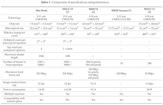
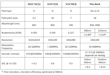
Although the press release does not mention any technical specifications it may be worth referring to an ISSCC paper from 2020 published by a team from Artilux that described a Ge-on-Si technology. The paper is titled "An Up-to-1400nm 500MHz Demodulated Time-of-Flight Image Sensor on a Ge-on-Si Platform" (https://doi.org/10.1109/ISSCC19947.2020.9063107).


Press Release: https://www.artiluxtech.com/resources/news/1014


Go to the original article...

Telluride Neuromorphic Workshop 2022

Image Sensors World        Go to the original article...

The 2022 edition of the Telluride Neuromorphic Workshop series will be held in-person June 26 to July 16 in beautiful Telluride, Colorado. The topics of interest are broadly in "neuromorphic engineering" with neuromorphic vision sensors (including event cameras and other "spiking"-based vision sensors) being key areas of interest.

Neuromorphic engineers design and fabricate artificial neural systems whose organizing principles are based on those of biological nervous systems. Over the past 27 years, the neuromorphic engineering research community focused on the understanding of low-level sensory processing and systems infrastructure; efforts are now expanding to apply this knowledge and infrastructure to addressing higher-level problems in perception, cognition, and learning. In this 3-week intensive workshop and through the Institute for Neuromorphic Engineering (INE), the mission is to promote interaction between senior and junior researchers; to educate new members of the community; to introduce new enabling fields and applications to the community; to promote ongoing collaborative activities emerging from the Workshop, and to promote a self-sustaining research field.

The workshop will be organized in four topic areas

  • Neuromorphic Tactile Exploration (Enhance the tactile exploration capabilities of robots)
  • Lifelong Learning at Scale: From Neuroscience Theory to Robotic Applications (Apply neuro-inspired principles of lifelong learning to autonomous systems.)
  • Cross-modality brain signals: auditory, visual and motor 
  • Neuromorphics Tools, Techniques and Hardware (SpiNNaker 2 and FPAAs)

Researchers from academia, industry and national labs are all encouraged to apply... 

... in particular if they are prepared to work on specific projects, talk about their own work or bring demonstrations to Telluride (e.g. robots, chips, software). 

An application is required to attend, and financial support is available. Application deadline is April 8, 2022.

Call for applications.

Application submission page.

Go to the original article...

Privacy-Aware Cameras for Human Pose Recognition

Image Sensors World        Go to the original article...

Carlos Hinojosa, Juan Carlos Niebles and Henry Arguello published an article titled "Learning Privacy-preserving Optics for Human Pose Estimation" in the 2021 International Conference on Computer Vision which was held virtually in October 2021. This is a collaboration between Universidad Industrial de Santander (Colombia) and Stanford University (USA).


The widespread use of always-connected digital cameras in our everyday life has led to increasing concerns about the users’ privacy and security. How to develop privacy-preserving computer vision systems? In particular, we want to prevent the camera from obtaining detailed visual data that may contain private information. However, we also want the camera to capture useful information to perform computer vision tasks. Inspired by the trend of jointly designing optics and algorithms, we tackle the problem of privacy-preserving human pose estimation by optimizing an optical encoder (hardware-level protection) with a software decoder (convolutional neural network) in an end-to-end framework. We introduce a visual privacy protection layer in our optical encoder that, parametrized appropriately, enables the optimization of the camera lens’s point spread function (PSF). We validate our approach with extensive simulations and a prototype camera. We show that our privacy-preserving deep optics approach successfully degrades or inhibits private attributes while maintaining important features to perform human pose estimation.


They take a "deep-optics" approach --- a learning-based approach where a neural network is used not only to recognize the human pose, but also to train a privacy-preserving point-spread-function (PSF). The neural network is trained to strike a balance between two competing requirements: (a) hiding scene information so that people's faces are not recognizable in the RGB images (even after image deblurring), while ensuring that (b) the PSF distortions aren't so strong that the pose-estimation task becomes impossible.


Their results look quite promising, and they even built a proof-of-concept hardware prototype using a wavefront modulator. Notice that the human faces are not recognizable in the RGB images, but the "match-stick" skeletons are still reliably picked out by the algorithm.


More details are in the open access paper and accompanying supplementary document and video available here: https://carloshinojosa.me/project/privacy-hpe/ 

Go to the original article...

Privacy-Aware Cameras for Human Pose Recognition

Image Sensors World        Go to the original article...

Carlos Hinojosa, Juan Carlos Niebles and Henry Arguello published an article titled "Learning Privacy-preserving Optics for Human Pose Estimation" in the 2021 International Conference on Computer Vision which was held virtually in October 2021. This is a collaboration between Universidad Industrial de Santander (Colombia) and Stanford University (USA).


The widespread use of always-connected digital cameras in our everyday life has led to increasing concerns about the users’ privacy and security. How to develop privacy-preserving computer vision systems? In particular, we want to prevent the camera from obtaining detailed visual data that may contain private information. However, we also want the camera to capture useful information to perform computer vision tasks. Inspired by the trend of jointly designing optics and algorithms, we tackle the problem of privacy-preserving human pose estimation by optimizing an optical encoder (hardware-level protection) with a software decoder (convolutional neural network) in an end-to-end framework. We introduce a visual privacy protection layer in our optical encoder that, parametrized appropriately, enables the optimization of the camera lens’s point spread function (PSF). We validate our approach with extensive simulations and a prototype camera. We show that our privacy-preserving deep optics approach successfully degrades or inhibits private attributes while maintaining important features to perform human pose estimation.


They take a "deep-optics" approach --- a learning-based approach where a neural network is used not only to recognize the human pose, but also to train a privacy-preserving point-spread-function (PSF). The neural network is trained to strike a balance between two competing requirements: (a) hiding scene information so that human aces are not recognizable in the RGB images (even after image deblurring), while ensuring that (b) the PSF distortions aren't so strong that the pose-estimation task becomes impossible.


Their results look quite promising, and they even built a proof-of-concept hardware prototype using a wavefront modulator. Notice that the human faces are not recognizable in the RGB images, but the "match-stick" skeletons are still reliably picked out by the algorithm.


More details are in the open access paper and accompanying supplementary document and video available here: https://carloshinojosa.me/project/privacy-hpe/ 

Go to the original article...

New Author Introduction – Atul Ingle

Image Sensors World        Go to the original article...

Atul Ingle has kindly agreed to help me publishing the posts and also give his unique view on image sensor from computer vision developer point of view.

Atul Ingle is an Assistant Professor in the Department of Computer Science at Portland State University. His research interests are in the fields of computational imaging, computer vision and signal processing. His current research involves co-design of imaging hardware and algorithms for single-photon image sensors. More broadly, he is interested in both passive and active 3D imaging applications that are severely resource-constrained in terms of power, bandwidth, and compute. Atul holds a PhD in Electrical and Computer Engineering from University of Wisconsin-Madison.

Go to the original article...

New Author Introduction – Saleh Masoodian

Image Sensors World        Go to the original article...

I'd guess many of you know Saleh Masoodian, CEO of Gigajot. I'm happy to announce that Saleh has kindly agreed to join the authors of the blog.

With Mark and Saleh, the new blog would offer quite diverse views on the industry.

Go to the original article...

Fujifilm INSTAX mini EVO review

Cameralabs        Go to the original article...

The INSTAX mini EVO is a digital instant camera with a screen and a built-in printer to make physical copies. It can also be used as a wireless printer for your phone. But does it lack the vintage charm we know and love from analogue INSTAX cameras? Find out in my review!…

Go to the original article...

Optimizing Machine Vision Lenses For Different Wavelengths

Image Sensors World        Go to the original article...

 Quality Magazine publishes an article covering consideration when Optimizing Machine Vision Lenses For Different Wavelengths.

"Lenses play a crucial role in the quality of the images produced by a machine vision system since they determine the sharpness of the image on the camera sensor. Lenses can influence image quality in a variety of ways:
  • Reduced light transmission due to lens surface reflections
  • Spherical, chromatic and defect aberrations preventing all rays of light from a single point on the object being focused to a single point on the image
  • Reduced light intensity towards the edge of the image
  • Spatial distortion of the image

By choosing the appropriate lens construction, all of these effects can be minimized. This article highlights some of the considerations when selecting a lens for your particular needs."


Go to the original article...

New Author Introduction – Mark Sapp

Image Sensors World        Go to the original article...

Dear Image Sensors World Blog readers,

Let me introduce Mark Sapp who kindly offered a help with posting the image sensor news in the blog. Mark is an electrical engineer working in the industry for 15 years and an enthusiast for cutting edge imaging technology, located in Austin, Texas. Mark, welcome to the community!

If somebody wants to post more news in the blog, please let me know and I'd gladly add you to the list of authors. I hope that this enriches the blog content and add more diverse views from the different branches of the industry.

Go to the original article...

Suspension of the Blog

Image Sensors World        Go to the original article...

Due to a large workload, I'm unable to continue publishing the blog. So, the blog is suspended for the time being.

Go to the original article...

303-Megaframes-per-Second Image Sensor

Image Sensors World        Go to the original article...

MDPI starts publishing a Special Issue on Recent Advances in CMOS Image Sensor with a paper "A Dual-Mode 303-Megaframes-per-Second Charge-Domain Time-Compressive Computational CMOS Image Sensor" by Keiichiro Kagawa, Masaya Horio, Anh Ngoc Pham, Thoriq Ibrahim, Shin-ichiro Okihara, Tatsuki Furuhashi, Taishi Takasawa, Keita Yasutomi, Shoji Kawahito, and Hajime Nagahara from Shizuoka University and Osaka University.

"An ultra-high-speed computational CMOS image sensor with a burst frame rate of 303 megaframes per second, which is the fastest among the solid-state image sensors, to our knowledge, is demonstrated. This image sensor is compatible with ordinary single-aperture lenses and can operate in dual modes, such as single-event filming mode or multi-exposure imaging mode, by reconfiguring the number of exposure cycles. To realize this frame rate, the charge modulator drivers were adequately designed to suppress the peak driving current taking advantage of the operational constraint of the multi-tap charge modulator. The pixel array is composed of macropixels with 2 × 2 4-tap subpixels. Because temporal compressive sensing is performed in the charge domain without any analog circuit, ultrafast frame rates, small pixel size, low noise, and low power consumption are achieved. In the experiments, single-event imaging of plasma emission in laser processing and multi-exposure transient imaging of light reflections to extend the depth range and to decompose multiple reflections for time-of-flight (TOF) depth imaging with a compression ratio of 8× were demonstrated. Time-resolved images similar to those obtained by the direct-type TOF were reproduced in a single shot, while the charge modulator for the indirect TOF was utilized."

Go to the original article...

Pixel Crosstalk in 2-Layer Sensors

Image Sensors World        Go to the original article...

MPDP publishes a paper "Parasitic Coupling in 3D Sequential Integration: The Example of a Two-Layer 3D Pixel" by Petros Sideris, Arnaud Peizerat, Perrine Batude, Gilles Sicard, and Christoforos Theodorou from University Grenoble Alpes which is the extended version of the paper presented at 10th International Conference on Modern Circuits and Systems Technologies (MOCAST), Thessaloniki, Greece, 5–7 July 2021.

"In this paper, we present a thorough analysis of parasitic coupling effects between different electrodes for a 3D Sequential Integration circuit example comprising stacked devices. More specifically, this study is performed for a Back-Side Illuminated, 4T–APS, 3D Sequential Integration pixel with both its photodiode and Transfer Gate at the bottom tier and the other parts of the circuit on the top tier. The effects of voltage bias and 3D inter-tier contacts are studied by using TCAD simulations. Coupling-induced electrical parameter variations are compared against variations due to temperature change, revealing that these two effects can cause similar levels of readout error for the top-tier readout circuit. On the bright side, we also demonstrate that in the case of a rolling shutter pixel readout, the coupling effect becomes nearly negligible. Therefore, we estimate that the presence of an inter-tier ground plane, normally used for electrical isolation, is not strictly mandatory for Monolithic 3D pixels."

Go to the original article...

Sony UV Image Sensor Video

Image Sensors World        Go to the original article...

Sony publishes a promotional video about its IMX487 UV sensor:

Go to the original article...

css.php