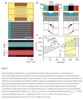
Image Sensors World Go to the original article...
Toulouse University publishes a PhD thesis "Developing a method for modeling, characterizing and mitigating parasitic light sensitivity in global shutter CMOS image sensors" by Federico Pace."Though being treated as a figure of merit, there is no standard metric for measuring Parasitic Light Sensitivity in Global Shutter CMOS Image Sensors. Some measurement techniques have been presented in literature [Mey+11], though they may not apply for a general characterization of each pixel in the array. Chapter 4 presents a development of a standard metric for measuring Parasitic Light Sensitivity in Global Shutter CMOS Image Sensors that can be applied to the large variety of Global Shutter CMOS Image Sensors on the market.
The metric relies on Quantum Efficiency (QE) measurements, which are widely known in the image sensor community and well standardized. The metric allows per-pixel characterization at different wavelength and at different impinging angles, thus allowing a more complete characterization of the Parasitic Light Sensitivity in Global Shutter CMOS Image Sensors."