Image Sensors World Go to the original article...
Soitec Capital Market Day presentation shows the company's innovations in wafers for imaging:


Visual Industry Guide
Image Sensors World Go to the original article...
Soitec Capital Market Day presentation shows the company's innovations in wafers for imaging:
Image Sensors World Go to the original article...
The AUTOVISION Spearhead Project aims to develop a graphene-based SWIR image sensor, and integrate it in a suitable camera system for self-driving cars.
Led by Qurv in Barcelona, AUTOVISION counts on the collaboration of industrial partners such Aixtron in the UK and Veoneer in Sweden, to help make safe deployment of autonomous vehicles possible.
The AUTOVISION project, over the course of three years, will produce CMOS graphene quantum dot image sensors in prototype sensor systems, ready for uptake in the automotive sector. Across the duration of the project, the developing image sensor is set to take huge leaps in sensitivity, operation speed and pixel size.

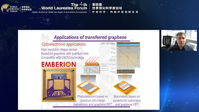
Image Sensors World Go to the original article...
Hamamatsu presents Lightsheet Readout Mode for microscopes that is said to improve image quality:
Image Sensors World Go to the original article...
Here is my list of the most significant achievements in image sensor industry this year:Image Sensors World Go to the original article...
Tencent, Sohu: Smartsens reports that in 2021 it has released 36 new products to mass production, and completed 31 tapeouts of future products including 4K and 8K image sensors for security and surveillance applications.


In a separate announcement, Smartsens presents its new automotive sensors: VGA SC031AP and 1MP SC101AP, both integrated with ISP and Tx output port:


Image Sensors World Go to the original article...
IEEE TED publishes Panasonic paper "Nonlinear Carrier Dynamics in a Single Photon Avalanche Diode: Stability, Bifurcation, and Quenching Condition" by Akito Inoue and Yutaka Hirose.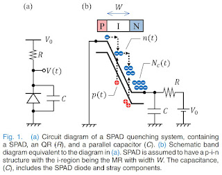
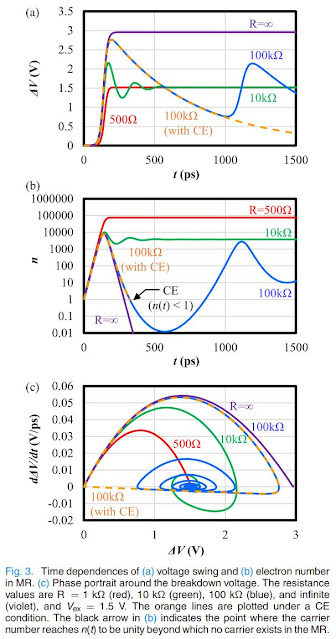
Image Sensors World Go to the original article...
BusinessWire: Stratio will work with South Korea’s National IT Industry Promotion Agency (NIPA) to create a first-of-its kind app that detects design infringements. The app instantly matches photos of suspected items to similar designs from an IP database to obtain a similarity score. This is possible through a backend which utilizes several of Stratio's imaging technologies, including algorithms for object detection, image retrieval, and report generation.

Image Sensors World Go to the original article...
JW Insights publishes a list of top R&D spenders among semiconductor companies in China. Image sensor companies Will Semi (Omnivision) and Goodix take 3rd and 5th places respectively:


Image Sensors World Go to the original article...
Canon publishes a press release about its SPAD sensor with 6.39 μm pixels presented at IEDM 2021: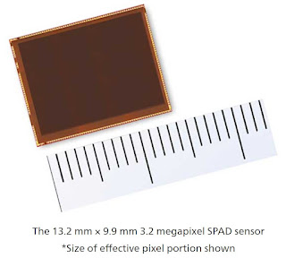
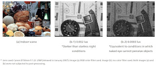

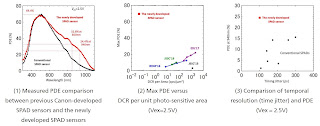
Image Sensors World Go to the original article...
ITHome, GizomoChina, Huaweiupdate: Huawei semiconductor division HiSilicon presents its Yueying ISP at China International Social Public Safety Expo (China Security Expo for short).


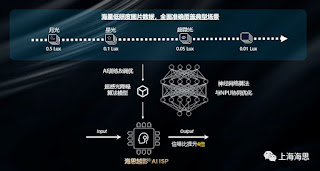
Image Sensors World Go to the original article...
ITHome, GizomoChina, Huaweiupdate: Huawei semiconductor division HiSilicon presents its Yueying ISP at China International Social Public Safety Expo (China Security Expo for short).Image Sensors World Go to the original article...
Omnivision publishes a series of milestone videos summarizing the company's progress over the years:Image Sensors World Go to the original article...
SigmaIntell publishes its report on camera module prices in China and its forecast for Q1 2022: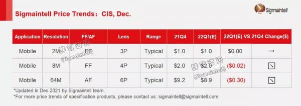
Image Sensors World Go to the original article...
Omnivision opens Howard Rhodes Lifetime Achievement Memorial Wall in its visitor center in Santa Clara, CA:
Image Sensors World Go to the original article...
Association for Advancing Automation (A3) publishes its list of "Image Sensor Innovations that Push Machine Vision Forward."
Image Sensors World Go to the original article...
ST publishes an article about its recent IEDM paper "1.62µm Global Shutter Quantum Dot Image Sensor Optimized for Near and Shortwave Infrared" by Johnathan Steckel: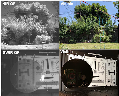

Image Sensors World Go to the original article...
MDPI publishes a review paper "Metasurface Photodetectors" by Jinzhao Li, Junyu Li, Shudao Zhou, and Fei Yi from Huazhong University of Science and Technology, National University of Defense Technology, and Raytron (China).
"Typical photodetectors only convert the intensity of light electrical output signals, leaving other electromagnetic parameters, such as the frequencies, phases, and polarization states unresolved. Metasurfaces are arrays of subwavelength structures that can manipulate the amplitude, phase, frequency, and polarization state of light. When combined with photodetectors, metasurfaces can enhance the light-matter interaction at the pixel level and also enable the detector pixels to resolve more electromagnetic parameters. In this paper, we review recent research efforts in merging metasurfaces with photodetectors towards improved detection performances and advanced detection schemes. The impacts of merging metasurfaces with photodetectors, on the architecture of optical systems, and potential applications are also discussed."


Image Sensors World Go to the original article...
Gpixel announces GMAX3809 extending the GMAX family into ITS applications next to its traditional industrial inspection segment. Gpixel optimized the GMAX product architecture with dedicated ITS features such as enhanced NIR response, pixel size of 3.8 μm, LED flicker mitigation and multiple region HDR modes. GMAX3809 is first in a series of GMAX products with optimized product features for ITS applications.
GMAX3809 fits 4096(H) x 2160(V) (9 MP) resolution into a 1.1” format with low noise, charge domain Global Shutter pixels running at 65 fps at 12-bit ADC resolution. GMAX3809’s 3.8 μm pixel achieves a FWC of 11.5 Ke- and noise of 3.6 e- which delivers more than 70 dB linear DR. The peak QE is 60%, a Parasitic Light Sensitivity is -92 dB, and angular response at > 15° is 80%.
GMAX3809 comes standard in a NIR-enhanced version using Gpixel’s Red Fox technology, offering the ultimate balance between NIR sensitivity and MTF. GMAX3809 achieves a QE of more than 30% at 850 nm and 14% at 940 nm.
GMAX3809 delivers 65 fps with 8 pairs of sub-LVDS channels each running at 960 Mbps resulting in a maximum data rate of 7.68 Gbps. On-chip functions, such as on-chip color offset calibration, channel multiplexing, multiple region HDR and LED flicker are available and programmable through SPI or I2C interface.
GMAX3809 is housed in a 163-pin ceramic LGA package with outer dimensions of 27.1 mm x 17.9 mm. The sensor assembly includes a double side AR coated cover glass lid.
GMAX3809 engineering samples can be ordered today for delivery in January, 2022.
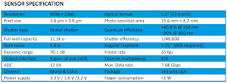
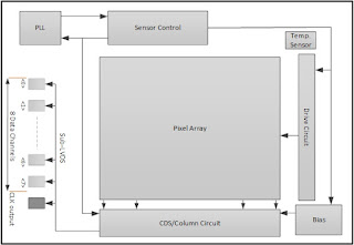
Image Sensors World Go to the original article...
Sina Technology: BYD Semiconductor's 1/15-inch 80,000-pixel CMOS sensor BF30A2 won the 2021 "China Chip" product award for outstanding market performance in the field of home appliances.
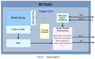
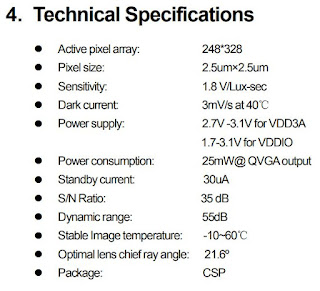
Image Sensors World Go to the original article...
Sina Technology: BYD Semiconductor's 1/15-inch 80,000-pixel CMOS sensor BF30A2 won the 2021 "China Chip" product award for outstanding market performance in the field of home appliances.Image Sensors World Go to the original article...
Photonics Spectra magazine holds is 2022 conference on January 10-13. Registration is free and available here. There are several image sensor presentations at this virtual event:Image Sensors World Go to the original article...
Light Co. publishes a video presenting its automotive stereo camera advantages over LiDAR featuring Guidehouse Principal Analyst Sam Abuelsamid, VP at Co-pace Continental AG Anil Rachakonda, Light CEO Dave Grannan, and Light's Chief Product Officer Prashant Velagaleti:
Politecnico di Milano publishes Harvard University's Federico Capasso lecture "Meta Optics: From Flat Lenses to Structured Light and Dark:"
Sony publishes 3 videos on its Pregius S stacked global shutter sensors (1, 2, 3):
Image Sensors World Go to the original article...
PRNewswire: TriEye announces "the first of its kind VCSEL powered Electro-Optic (EO) SWIR system", integrating TriEye CMOS-based sensor with VCSEL as an illumination source.
TriEye demonstrates an EO system by integrating the TriEye Raven with 1350nm SWIR VCSEL-based illumination, provided by their VCSEL partner, as such they enable the highest power density - which today is over 5 watts per mm2 . This new EO system will provide significant value for short-range applications such as mobile, biometrics, industrial automation, medical and more.
TriEye's solution is said to be the first to provide SWIR based sensing using VCSEL technology. TriEye's SWIR system opens doors to next generation perception capabilities by providing a significant value proposition compared to the NIR spectrum. This includes resilience to sunlight and other sources of ambient noises while providing an eye-safe illumination source. With this combination, the perception system will have longer range and better accuracy than previously achievable with NIR based systems.
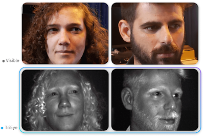
Image Sensors World Go to the original article...
NTT Device Technology Lab publishes an OSA Optica paper "Full-color-sorting metalenses for high-sensitivity image sensors" by Masashi Miyata, Naru Nemoto, Kota Shikama, Fumihide Kobayashi, and Toshikazu Hashimoto.
"Image sensors play a critical role in current technologies ranging from smartphones to autonomous vehicles. In these technologies, high-sensitivity image sensors are highly desired because they enable dark-scene/ultra-fast imaging. Unfortunately, a conventional sensor architecture that employs color filters on every pixel fundamentally limits the detected light power per pixel because of the filtering, which has been a long-standing barrier to sensitivity improvement. Here, we demonstrate polarization-insensitive metasurface lenses (metalenses) that sort primary colors on high-density pixels without the use of color filters. The metalenses simultaneously act as pixel-scale color splitters and lenses and are compatible with complementary metal–oxide-semiconductor sensor technology. An image sensor with such metalenses significantly enhances the detected light power, while affording high image quality, incident angle tolerance, and sub-micrometer spatial resolution. The demonstrated architecture opens the way to the development of high-sensitivity color image sensors that exceed current limits while maintaining consistency with state-of-the-art sensor technology."


Image Sensors World Go to the original article...
Abhiram Gnanasambandam and Stanley H. Chan from Purdue University publish Arxiv.org paper "Exposure-Referred Signal-to-Noise Ratio for Digital Image Sensors."
"The signal-to-noise ratio (SNR) of a digital image sensor is typically defined as the ratio between the mean over the standard deviation of the sensor's output, thus known as the output-referred SNR. For sensors with a large full-well capacity, the output-referred SNR demonstrates the well-known linear response in the log-log scale. However, as the input exposure approaches the full-well capacity, the vanishing randomness of the saturated pixel will cause this output-referred SNR to artificially go to infinity. Since modern digital image sensors have a small pitch and hence a small full-well capacity, the shortcomings of the output-referred SNR motivated the development of a theoretical concept known as the exposure-referred SNR, first reported in some sensors and computer vision papers in the 1990's and more since 2010. Some intuitions of the exposure-referred SNR have been discussed in the past, but little is known how the exposure-referred SNR can be rigorously derived.
Recognizing the significance of such an analysis to all present and future small pixels, this paper presents a theoretical analysis to justify the definition and answer four questions:
(1) What is the correct definition of SNR?
(2) How is the output-referred SNR related to the exposure-referred SNR?
(3) For simple noise models, the SNRs can be analytically derived, but for complex noise models, how to numerically compute the SNR?
(4) What utilities can the exposure-referred SNR bring to solving imaging tasks?
New theoretical results are shown to confirm the validity of the exposure-referred SNR for image sensors of any bit-depth and full-well capacity."


Image Sensors World Go to the original article...
2022 Electronic Imaging Symposium is to be held on-line starting January 16. There is a number of image sensor presentations:Image Sensors World Go to the original article...
ams OSRAM is expanding its portfolio of dToF modules with three new devices for multi-zone and multi-object detection with a wider FoV and extended range. The multi-zone dToF modules TMF8820, TMF8821, and TMF8828 allow for a precise distance measurement.
The TMF8820 divides the FoV into 3x3 or 9 individual detection zones, the TMF8821 into 4x4 or 16 individual detection zones and the TMF8828 into 8x8 or 64 individual detection zones. With multi-zone detection, it is possible to identify where an object is located within the sensors FoV. These new devices feature a dynamically adjustable FoV up to 63°, enabling customers to select either a narrow or wide FoV to meet their application needs. All th
ree dToF modules have a detection range from one centimeter up to five meters.
The modules combine a 940 nm VCSEL, a SPAD array with matching multi-lens optics, and an on-chip microcontroller for histogram processing in one device. Thanks to the compact dimensions of 2.0 mm x 4.6 mm x 1.4 mm, the modules are said to be the smallest multi-zone dToF modules available on the market.


Image Sensors World Go to the original article...
Sony presents IEDM paper on pixel level stacked sensor with 2-Layer Transistor Pixel. Whereas conventional CMOS image sensors’ photodiodes and pixel transistors occupy the same substrate, Sony’s new technology separates photodiodes and pixel transistors on different substrate layers. This is said to double saturation signal level relative to conventional image sensors, widen DR and reduce noise. The new technology’s pixel structure will enable pixels to maintain or improve their existing properties at not only current but also smaller pixel sizes.

